Wednesday, December 27, 2017

YAC, a DAC (floating point)

I started looking for Yamaha OPL2 (YM3812) and OPL3 (YMF262) chips on ebay yesterday, as I thought it would be nice to get some for future use. These vintage FM chips were everywhere in the late 80's and early 90's, particularly on Adlib and SoundBlaster sound cards.

I soon realised that one needs an additional chip - a DAC - as the chips are completely digital.

The DACs used are YM3014B for the OPL2 and YAC512 for the OPL3. Both are serial input DACs with what they call 16bit dynamic range. But they are not 16bit integer DACs. So what are they?

They are in fact floating point DACs, with one "normal" integer DAC (10bit), called the mantissa, and an exponential multiplier, the exponent, that sets the reference voltage. This is just like a floating point number which has a significand (the mantissa) and a base raised to the power of an exponent.

As the exponent changes, the width of each step of the 10bit DAC changes. This means that at the resolution is higher at the lower end of the scale, and it decreases (the step width increases) as one moves upwards.

The circuitry is presumably along the lines of this (though this patent is from 1990 and the YM3014B is much older than that), though the Yamaha datasheets call the exponential part an analog shifter:
Floating point DAC patent
The YAC512 supports two time multiplexed outputs from a single DAC through external sample and hold capacitors. The YM3014B is single channel and requires no sample and hold.

I wonder if it would be a good idea to use such a DAC for my DCO - it seems to be available for less than $1 a piece on ebay, though I'm not sure if those are fakes or not. The exponential nature of the DAC should fit an exponential scale well.

Sunday, November 5, 2017

JP6 vs Juno 106 filters - Hz per mA

NB: This post was written before i discovered a missing 33k feedback resistor. Results may not be correct.

I've simulated both the Juno 106 filter (with 270pF caps) and the JP6 filter in 24dB LP mode, to figure out their response - what voltage (or rather current) to frequency rate to expect.

Quite interestingly, the two implementations track each other fairly well. Both have around a 30Hz per mA or 30uA per Hz response.

EDIT 26/12-18: It seems I've messed up a bit? (0.1V / 3300Ohm ) / 4 is not 7.57mA, it's 7.57uA. Thus the response is 30Hz/uA or 30nA/Hz?

Also very interesting to note is that the response is not linear. The higher the frequency, the more current is needed for the same change in Hertz.

I measured the 3dB point at 16 selected currents:


The CV is the input to a constant current circuit. It is the voltage across a 3k3 resistor, and the resulting current (buffered to stay constant) is split between the four cells of the filters.

I selected 8 tightly spaced voltages and 8 further apart, as the lower end requires less change to double the frequency. Deltas are the difference between two measurements. F_c is the 3dB cutoff frequency point. This is a linear CV, e.g. without the exponential converter connected.

The result ended up like this:

Note that the y axis is truncated to get a better view of the effect. One would expect a linear response, but in fact, as mentioned, the Hz pr mA drops as the frequency increases. The Juno follows a sharper curve and even if it starts out higher than the JP, it drops below it at some point. In other words, the Juno linearity is worse than that of the JP.

So what does this mean? It means that the V/oct tracking of the filter is not perfect. It will be slightly more closed as one moves up the scale on the keyboard. I have read about this effect earlier, and the writer noted that it didn't seem to matter all that much. I guess a little difference is hard to hear when the base frequency changes a lot.

Wednesday, October 25, 2017

Jupiter 6 filter clone - initial simulation

After the success with simulating the juno filter, I tried the same with the Jupiter 6 multimode filter today. I struggled a lot before I got things up and running - among other things I forgot to connect the power to the resonance OTA of the first cell, and I never got the resonance control from the Jupiter 6 schematic to work so I swapped it for the one from the Juno.

After that however, things turned out VERY nice! What's interesting is that the circuit is exactly the one from the datasheet, with the same component values (replacing the OTAs with LM13700 without the output transistors, and using separate opamp buffers) - and the frequency response tracks the one from the juno clone very well. I got a slightly better tracking by switching from 330pF caps to 323pF, but 330pF will work just fine.

Here are a few plots before I go into details about some discoveries. The output VCA has been tweaked to give us a 0dB output for pass frequencies of the 24dB low pass filter>

This first one shows the frequency response of four of the five possible variations of the two cells. Here the LP output of the first stage is connected to the second stage:


  • Red is LP (12dB) + LP (12dB), or a 24dB LP
  • Green is 12dB LP tapped after the first stage
  • Blue is 12dB HP tapped after the first stage
  • Turquoise is 12dB LP + 12dB HP, or a 12dB BP


In the second one I've connected the HP output from the first stage to the second stage


  • Red is 12dB HP + 12dB LP, or a 12dB BP, similar to the option from plot 1
  • Green is 12dB LP tapped after the first stage
  • Blue is 12dB HP tapped after the first stage
  • Turquoise is 12dB HP + 12dHP, or a 24dB HP


The -3dB cutoff (for the 24dB LP filter) is at 727Hz (measured)


As for the discoveries: For a long time I could not get rid of the resonance. I even tried changing the feedback resistors that tap the stages and send them to the resonance OTAs, but it just didn't want to go away. But then I realised that I had forgotten to connect power to one of the resonance OTAs.

So what did I learn from this? Well, without the resonance OTA, the circuit actually self-oscillates. By adding parts of the signal tapped after the first 6dB cell, we cancel out the feedback that leads to oscillation (or at least that's what I think happens).

This leads to another realization - the control signal for the resonance is reversed. In the Juno, 0V of resonance CV turns off resonance and it increases the closer to 10V we get (also, I think the transistor in the Juno resonance CV circuit acts as an exponential converter, but I have not checked this). In the Jupiter 6 filter, when using the same resonance control circuit, 0V gives a huge (80dB) spike!

Maximum resonance


At 10V resonance is fully turned off. I have yet to confirm that 10V is indeed the correct max voltage for turning off resonance, but with this setting the plot looks exactly like it does for the juno with resonance CV=0V

Oh, and as a closing note - turning up the resonance does NOT attenuate pass frequencies. In the Juno, frequencies below the peak are attenuated up to 8-10dB - but more of that in a separate post comparing the two filters. I'll also post the circuit and work out the necessary control circuitry to get 1V/octave responses for the cutoff, but that's for later.

Update: I just came across a Jupiter 6 filter clone, I belive it is by the guy that writes at polysynth.blogspot.com. It says that the clone is open source, but for my own sake and the fun of working things out by myself, I'll try as hard as I can to not look at his clone before I finish mine :-D

Tuesday, October 24, 2017

BA662 clone

While studying the Juno 106 filter I came across Analogue Renaissance's BA662 clone. It is dirt simple, but when I tried simulating it, I got massive distortion on the output compared to my Xonik linear VCA (based on the research by bergfotron etc, see separate post on the VCA)

When running a 2V p-p signal through it, using a 0.110mA (15V/136k) control current I got an output signal with the same amplitude, but the sine wave had been visibly distorted. Suspecting that this was only a simulation problem, I tried breadboarding the circuit. The distortion was even more visible on the oscilloscope.

2V p-p input (green), distorted output (blue)

I quickly realised that the amplification was not linear close to the maximum signal amplitude, much like a compressor/limiter circuit. Reducing the input to 1V p-p showed that the gain was in fact not 1 but more like 1.5.

Adjusted input, 1V p-p
After readjusting the control current to get unity gain again, I could still see some distortion:

Adjusted amplitude. Output wave is still distorted, though not as much as earlier

After reducing the input further, to 0.5V p-p, and readjusting the control current again, I got this, which seems much better. The control current is now 61.9uA


Then I took a closer look at a document I printed a few years back, that shows what voltages and currents to expect in the Juno:

An annotated Juno 106 service manual showing the various voltages. I can't quite remember where I got it, but I THINK Analogue renaissance made it?

To see how the BA662 is actually used in the circuit, I added the resistors between VCF out and VCA in (though not the VCA offset pot) and set the pot to 25k. Without changing the control current I got this:

Clone as used in the Juno 106 - with the 50k pot centered. Ampitude is MUCH lower.

Notice the significantly lower amplitude. I then adjusted the control current to the maximum according to the document above and got this:

Same configuration but with the control current at 0.3mA, which according to the picture above is the maximum. Notice that the amplitude is alost a quarter of the input. Even if we increase the control current, we are unable to reach unity gain.
So, there is no way to get unity gain out of this. I guess it is compensated elsewhere in the circuit. What troubles me is that with that much attenuation, wouldn't the VCA be unnecessarily noisy?

I will have to recheck the Xonik Linear VCA to see it it suffers from the same distortion problems. From my notes I see that I run it using a control current up to 1.5mA.

Juno filter analysis

I intend to use the Jupiter 6 multi mode filter for the XM8. As this is based on the IR3109, just like the Juno 6/60/106, which is better documented, I took a closer look at that filter first.

Analogue renaissance delivers a great clone of the 106 filter. I am not trying to build a drop-in replacement for anything, so exact component values to match the Juno's are not important, but the idea of using LM13700 in place of the IR3109's OTAs seem to be the go-to solution these days.

In fact, for the filter part (ignoring the resonance and output VCA), part values are mostly the same between the clone and the original Juno 6/60 circuit - 560R and 68k resistors all the way. The caps are 270p in the clone and 240 in the Juno 6/60. I have done a thorough comparison between the various IR3109 filter circuits made by Roland, most of them use 560/68k resistors. The caps have changed from 240p in earlier designs to 330p in later. It probably only affects the exact cutoff-to-CV; I'll test this before I decide on the cap value to use.

I wondered what the linear CV response of the filter would be, so I simulated the circuit in LT-spice. NB: This is the first time I do anything like this, so my findings may not be correct. However, it seems that the current is the case:

For every 2.5kHz increase, the OTA control current increases by 75uA. This means that the LINEAR control current to frequency ratio is (100 * 10^6) / 3 Hz per A. It does not seem perfectly linear however, it drops off somewhat as we go up the scale (an increase from 75 to 150uA increases the frequency by 2,54kHz while an increase from 300 to 375uA increases the frequency by 2.31kHz.

Of course, to properly control the filter, an exponential converter or a DAC output with a high enough resolution is needed. A cutoff of 10Hz requires 0.3uA while 10kHz requires 300uA, a factor of 1000.

Similarly to the DCO frequency calculations, the feasibility of this has to be tested properly, and we may get issues with opamp inaccuracies at the lower end of the scale, though they may not be as severe as with the DCO because the error is not accumulated over time.

PS: The Juno 106 has non-polar caps in line with the signal both before and after the filter. These act as a highpass filter with cutoff around 10Hz.

Filter response with cutoff around 2.5kHz, with HPF included


Update: Replacing the 270p caps with 330p caps changes the control current-to-cutoff frequency from 2.5kHz/75uA to 2.1kHz/75uA, with the same slight dropoff as the frequency increases.

Sunday, October 15, 2017

Noise filter responses


I just downloaded LTspice IV in order to simulate filter responses for the state variable filter for the XM8. To learn, I started out by simulating the various noise filters from the Andromeda A6.

Here are some nice plots to look at (continuous line is frequency response, dashed is phase response):

The A6 noise circuit. I've used LT1001 opamps, just because they where the first in the list.
White noise filter - an HPF. Measured Fc seems to be around 5.3Hz; each of the two filters have an Fc of 3.43Hz. Gain is around 36dB (?)  (multiplier: 72)

Pink noise filter, a 3dB low pass filter approximation, fairly linear from 10Hz to 20kHz. Gain is around 26dB (multiplier around 19.6 measured, as opposed to 21 calculated from the normal non-inverting amplifier formula, due to the 68k resistor)

White and pink noise filters combined

Red noise filter, 12dB low pass with Fc at 107.6Hz. Gain is approx 10dB (multiplier: 3.16)

White, pink and red noise filters combined

Now, after simulating the A6, of course I had to do the same to my pro-one/elliot white/pink noise combination. It turned out like this:
Pro one modificaton white noise. This is an HPF, similar to the one from the A6. The gain is very different though, about 55dB for this one. 

The Elliot 3dB pink noise filter. Not very different from the A6, but with a very different phase change.

White and pink noise filters combined. Fairly similar to the A6.
Now for the interesting part - how do the two circuits compare? Well, first of all, the overall gain of the A6 is significantly less than the pro one/Elliot version. Here is a combined plot:


A6 (green) vs pro one/Elliot (blue).
I did however do a calculation of all expected gains and updated the A6 circuit with a 20k resistor in place of the first 2.43k one in the white noise circuit. It sounded very similar to the pro one/Elliot after that, but what do the plot look like?

A6 after replacing a resistor (green) vs pro one/elliot (blue)
I'd say they are very similar! One thing to notice though, is the difference at the deep end. The pro one/elliot removes much more of the really deep frequencies. This is below what your ear should be able to hear though.


Xonik Waveshaper v1.0

The wave shaper board and Noise board was sent off to DirtyPCBs for production last week. They both turned out rather nice - the waveshaper board measures 28 x 64 mm and the noise around 24 x 25 mm.

Interestingly enough, the sub oscillator circuit takes up more than half of the waveshaper due to the many options (-1/-2 octaves, saw or square wave).

I’ve tested the circuit with the DCO and got some very nice results. There are still some spikes on the sub saw waves, but while adding filter caps did reduce the spike amplitudes, it also widened their base. I’ve chosen to leave the spikes as is but have left room for the filter caps should I redecide.

The noise board requires four external trimmers - one to center the saw wave, one to trim the triangle and sine waves and two to match the saw wave parts in the sub oscillator.

The noise circuit requires an external noisy 2n3904 or, as in the Andromeda A6, 1N5237B/8.2V zener diode. It has the option of adding a trimmer to control the noise amplitude, but also has room to just use an on-board resistor if exact amplitude is not of essence.

The A6 uses an opamp to offset the noise outputs due to its internal offset center (PMID), which also acts as a filter. This is not included in my circuit.

Waveshaper board. All mixing and amplitude control must be done externaly which makes it possible to use this card both with computer control and directly with mechanical switches or potentiometers if one wants to make a mono synth without patch storage.


Here are some photos of the output when the XDCO is connected istead of a function generator:
Saw

Sub oscillator saw, one octave down

Sub oscillator saw, two octaves down

Inverse saw


Triangle
Sine
Square

Sub oscillator square, one octave down

Sub oscillator square, two octaves down

Pulse wave
The results look very good, but I have yet to run it with a amplitude calibrated DCO, so right now wave shaping is not perfect for all frequencies, only the one the waveshaper is manually calibrated for.

Sunday, October 1, 2017

Xonik DCO v1.0

The XDCO board arrived friday, and yesterday I soldered one to test it. I cannot find my 2N3904 SMD transistors for some reason, I was supposed to have received 100 of them in my last Farnell shipment but they were nowhere to be found. Instead, I had to modify a regular 2N3904 to fit the SMD footprint. It works fine but looks rather strange - and is of course not very durable. But for testing, it works just fine.

This wouldn't be a real Xonik project if the first version worked flawlessly however. After some initial problems programming the chip (I connected ISCP data and clock to SPI data and clock....), I discovered that I've used ISCP data as DCO CS, and NOT exposed it as a separate pin! That means that it is not possible to program the chip in circuit. I had to add a thin wire to expose pin 13 on the MCU. After doing this, everything worked as planned and I now have a working DCO.

The ISCP bug may be handled two ways:
- fix the bug and re-order the boards
- develop a boot loader and program the chips before soldering them into the circuit, then use SPI for programming later.

I've wanted to do a boot loader for a long time, so maybe this is the motivation I need - we'll see. The price of the board is not a big issue, they cost less than $20.

As for the crystals and speed - On the breadboard the crystals didn't start properly, resulting in fallback to the internal oscillator. I bought new crystals and did some proper calculation on what caps to use (the crystals require 18pF, using two 27pF in series should result in the correct value, see separate post) and now the crystals oscillate at the desired 32MHz right from the start.

Time to test the DCO with the waveshaper!

Update:
While the frequency is ok, the amplitude is off. The output maxes out at around 8.6V. If removing the cap, we get a flat 8.6V meaning something sinks the rest (?).  I tried removing the transistor collector, the opamp saturated to 15V so it is absolutely capable of delivering the necessary voltage. I also tried disabling resetting of the cap and even then the max was the same. The output stays at 8.6V even while programming the circuit. Someting is definitely wrong around the transistor.

BTW: I tried 5 different transistor and three variants of opamps on the breadboard and it still worked fine.

Update 2:
The amplitude issue was just a miswiring of the external transistor, I had mixed up collector and emitter. After changing this, calibration works again. There are some issues with timing and mcu crashes though, maybe related to unfiltered psu lines?

I've also tested and eliminated the 330k resistor from base to ground. it is necessary in the Juno 6 to keep the base voltage between 1.5 and -12.5 (from a 0 to 5v input) to control a PNP transistor. I am using an NPN which is on when the base is > 0.7V and off when the base is at GND, so it can be controlled directly without any biasing resistor. I've also checked the 68k value, it keeps the I_base high enough to allow I_c to be fully sunk while still being low enough to not damage the transistor.

Monday, September 25, 2017

Xonik Waveshaper - breadboarded version

I finished breadboarding the waveshaper last night. Here is the schematics (not bug checked though) and a few photos of the output waveforms from the sub oscillator. The saw wave looks like crap but that is because I used a function generator without saw output as the source of the original wave (using a triangle wave with a very unbalanced center in place of the saw). It will look a great deal better with a real saw wave input.

Full waveshaper circuit. Note that the sub saw output has the same polarity as the input. It is also possible to get an inverted output.
Square wave (top) and square wave sub oscillator

Pulse wave and square wave sub oscillator

Saw wave and saw wave sub oscillator. Note that the spikes are artifacts created by the not-completely-a-saw-wave input (the vertical lines in the input wave are not fully vertical). This will disappear when using a real saw wave as input.

1 oct down and 2 oct down saw waves.


Sunday, September 24, 2017

Coming soon: the Xonik Waveshaper


On my breadboard today: The Xonik Waveshaper - insert a non-centered 0-10V saw wave from the Xonik DCO and you'll get the following (centered) waves:

- Saw
- Inverted saw
- Triangle
- Sine
- Pulse/square with VC-PWM and VC amplitude (no VCA needed)
- Sub oscillator with square -1oct, square -2 oct, saw -1 oct and saw -2 oct.

The current triangle/sine circuit is based on the Jupiter 8 and Yusynth modular, the sub oscillator is a simplified version of the Xonik Sub oscillator. The pulse circuit amplitude control idea (but not circuit) is lifted from the Juno.


Friday, September 22, 2017

Alesis Andromeda A6

While searching for noise samples to compare my breadboarded noise against, I had a look at the Andromeda A6 circuit diagram. It is fun to study what the big guys think are good designs and I've picked up a few ideas already. I will probably post more as I go anlong.

My first findings

Separate center reference voltage

The A6 seems to use a reference voltage, PMID/PDMID in place of ground whenever ground would be expected on any of the inputs of an opamp. My guess is that PMID/PDMID means Power Middle/Power Digital Middle or something like that, as ground in these places would normally be the center of the wave.

The PxMID originates with a 5V voltage regulator. I've calculated PxMID to be 2.05V. The A6 uses +/- 12V internally, with an offset of +2V this means that any positive amplitude is reduced to +10V minus any opamp limitations.

The PMID line is littered with bypass caps. I assume that by using a separate, well regulated reference voltage, one may get rid of some noise from other components, and also that its hard to get 0V from a regulator, thats why it's 2.05V (?).

Noise


The A6 has most of its analog circuitry inside a bunch of ASICs. The noise section however, is discrete. Only one noise source is used for all voices and it supplies white, pink and red noise.

The noise source seems fairly standard, it is based around a zener diode (which is the same technique as using a transistor without connecting the collector). The pink noise filter seems to be a true pink noise approximation (3dB/oct) as it uses a multiple filter sections in the same fashion as Elliot Sound Products. It is not entirely similar as it has the filter sections connected to between the positive input and ground, whereas the Elliot version have them in the feedback loop, but I assume this is only because the A6 one is a non-inverting filter and the Elliot an inverting filter. All noise outputs are connected to an inverting amp which also adds the PMID reference and acts as a low pass filter with cutoff at 493Hz.

Analog pots


All analog pots (that are read digitally) have 10nF caps across them - I assume this is to stabilize values or prevent that noise from one pot falsely triggers another one. 8 5kOhm pots are multiplexed through one CD4051 mux.

FX bus


The FX send has both positive and negative sends that are inverted versions of each other. Not sure if this means that it uses a balanced bus but it could be likely. Further investigation necessary :-D

Master volume


Master volume is a physical pot connected directly in the audio path, no VCA is used. No master volume saving is possible which makes sense.

Monday, September 11, 2017

Noise research

I intend for the XM8 to have noise as a waveform for both oscillators, and also to be able to switch between various 'colors' of noise. At the very least, white and pink noise should be present, possibly even red. But what exactly does this mean?

White noise is noise where the signal has equal intensity at all frequencies. In the synth world, it is commonly generated by using a transistor with one leg disconnected.

Pink noise is a signal where each octave carries the same amount of noise energy. But how is this achieved in practice?

According to Wikipedia, pink noise falls off at 3dB per octave. To get pink noise one filters white noise through a filter with 3dB/octave drop off.

Problem is, most basic active low pass filter has a 6dB drop off (which would actually give us red noise if used). So how may this be solved?

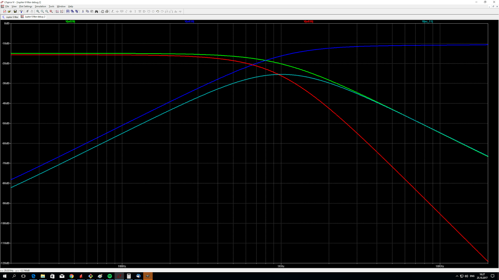
This page shows one method - use multiple filter sections to approximate a 3dB filter with a flat response. The more sections the better, but even four sections is pretty good for a 20-20 000kHz signal.

As a side note - the same page mentions NP capacitors, bipolar electrolytics, and says that film capacitors cannot replace them - this is interesting information as I've stumbled across NP in other circuits.

A similar approach seems to be in use on this page, which is a modification for the Sequential Circuits Pro One. It uses fewer sections (two?) and has an additional cap (C3).

But how does one calculate the frequency of each section?

In a normal active low pass filter (6dB), the frequency is 1/(2*PI*R2*C) and the gain is -R2/R1 where R2 is the resistor in the feedback loop.

It seems that the same holds true for each section in the multi section filter. For example:

1/6.28*100nF*1MOhm) = 1.59Hz
1/6.28*33nF*330kOhm) = 14.6Hz
...
which matches the frequencies next to the sections.

This would mean that the lower section of the Pro one filter is 338.8Hz, but the rest - the 270k and 3.3n combined gives us a 268.1Hz filter which seems a bit strange - however, I'm not sure this is the way to calculate the combined frequencies.

As for the gain, if the same formula as before is correct, it would be -270k/15k = -18.

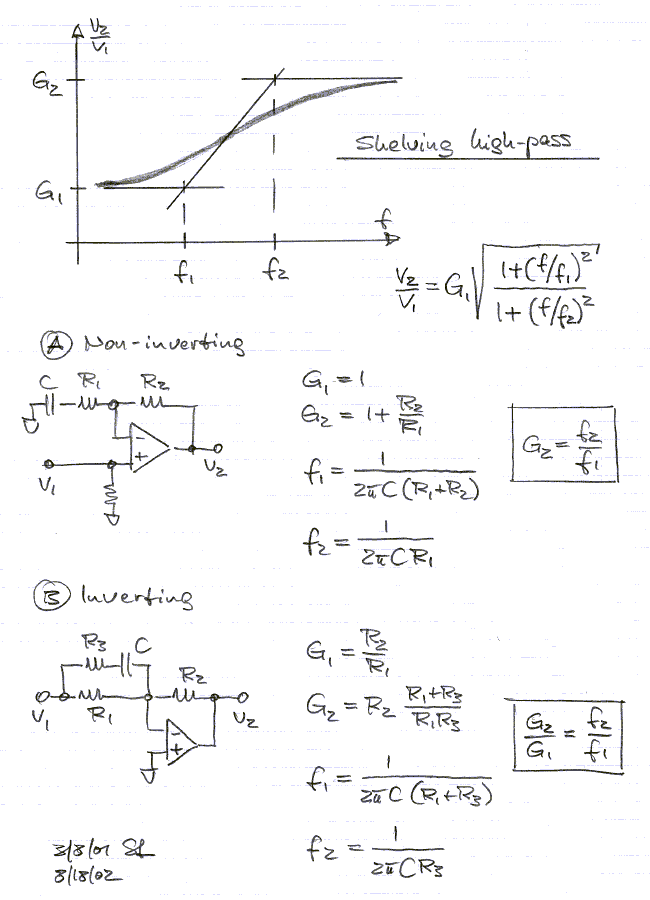
The pink noise filter in the pro one matches the inverting shelving low pass filter found on this page. However, the only formula, found in the gif, is missing the lone cap in the feedback circuit.

Funny enough, the same filter topology is found in the BOSS CE-2 pedal's de-emphasis filter :). The de-emphasis filter reduces treble, which of course means it is a low pass filter of sorts. :)

On that page, the circuit is fully explained. When calculating the frequencies, the lone cap is omitted. It says that it is an LP of some sort but it is not essential when calculating the shelving frequencies.

The filter right after the transistor in the pro one circuit is a simple non-inverting HP filter. C2 and U1b forms a shelving HP filter like this.

The first filter in the Ray Wilson Noise Cornucopia is a simplified non-inverting amplifier filter as shown here and here. Its gain is 1 + R10/R9 (=48), the frequency is 1/(2*PI*R10*C4), or approx 34kHz.

ERROR: det er et lowpass non inverting shelving filter.

Saturday, September 9, 2017

Wiring the Xonik PSU3 v1.0

The Xonik PSU3 v1.0 is a copy of the Ken Stone CGS66 Rev 1.1.

In addition to the dual voltage of the CGS66, it has a third part meant for digital/logic voltage.

The input to the third channel may either be a dual secondary/centre-tap transformer or a single secondary. If using a dual secondary, do NOT connect D11 and D12.

Using two transformers - connect earth to ground/0V on both connectors and mount D11 and D12

Using one transformer (or two centre-tap transformers): do NOT mount D11 and D12.
NB: Remember to fit suitable fuses and switches on the primary sides of the transformers.

The colors on the dual secondary transformer are the ones used on my Noratel TA050/15:


PS: The Xonik PSU3 has the main smoothing capacitors mounted close to the heat sinks. If the heat sinks get hot, the lifespan of the caps may be reduced.

On transformers and rectifiers

Everywhere that you find information about transformers, it says "make sure that you know what you do, these things can kill you".

Well, I thought I knew, but I still managed to mess up. I didn't get killed, but I learned a bit about transformers and rectifiers.


Let me explain.

There are two basic ways of turning an AC voltage into a DC voltage. One uses a half wave rectifier, the second a full wave rectifier.

The difference is that the half way rectifier only uses the positive part of the voltage swing, whereas the full wave rectifier uses both parts by magically reflecting the negative part. The full wave rectifier requires a few extra diodes but gives a smoother DC voltage (or at least one that requires a smaller smoothing capacitor and is more efficient).

Then there are two basic transformer configurations - single and dual secondary. When the two outputs of the secondary are of equal voltage, and the "bottom" of one is connected to the "top" of the next, we call it a centre-tap transformer. This kind of transformer is often used if you want a dual voltage output, for example +15V and -15V for audio circuits.

Here is how the different transformers may be connected for a single output voltage.

First off, a single secondary, half wave rectified configuration:

Here, the lower pin of the secondary is connected to ground, and the top is connected to a smoothing cap through a power diode.


Then we have the single secondary, full wave rectified configuration:

Here, none of the secondary output pins are connected to ground. Instead, they are connected to the top and bottom of a diode bridge rectifier. Then, one of the other rectifier junctions is connected to the smoothing cap, and the last one is connected to ground.


Now, if we have a centre-tap transformer, we get to use a little trick:

Instead of using four diodes, we get away with two. Ground is connected to the centre tap.


So what if we want a dual (positive and negative) output from a centre-tap transformer? Well, just duplicate the circuit, but turn the diodes the other way around for the second half.

This looks suspiciously like the full wave rectifier for the single secondary transformer, but there is a crucial difference!

Instead of connecting the last pole of the diode bridge to ground, it is used as the point where we tap the negative voltage/connect the smoothing cap for the negative voltage.

This may seem obvious, but when I tried to use a centre-tap transformer for a single output voltage, I didn't think this part trough. I left the four diodes in and connected both the last pole of the diode bridge AND the centre-tap to ground. This immediately blew the input fuses (luckily I was using fuses) and it is easy to see why: With the diodes in place there is a direct short (well, through the diodes anyway) between the negative half wave and ground, which drew a large current.


As for my circuit design - the fact that I both have a three pin input with one pin connected to ground, and room for four diodes in the bridge rectifier, means I can use both a centre-tap and single secondary transformer - as long as I do not connect the diodes when connecting the centre tap.