Before converting the JP6 filter to 12V, I wanted to know a bit more about what happens when changing the supply of the LM13700 from 15V to 12V. (For simplicity, throughout this text I will say 15V and 12V when I actually mean a +/-15V and +/-12V supply voltage).
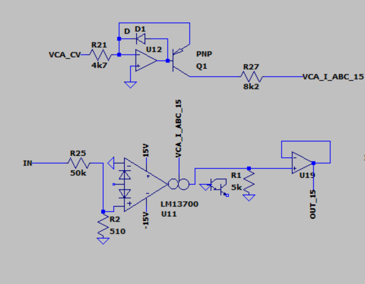
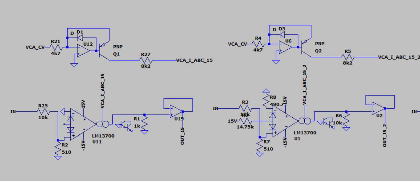
As a first model I used the Xonik VCA.
Xonik VCA
I first calibrated the circuit for unity gain at 5VCV, 15V supply, then updated it for 12V by replacing the diode bias resistor and doing slight changes to centering. (Actually, I made the 12V first then calculated a new diode bias resistor by first finding I_d as 11.3V / 12k = 0.942mA, then finding a new resistor as 14.3k / 0.942mA = 15.18k. The voltage across the resistor is said to be one diode drop away from the supply voltage).
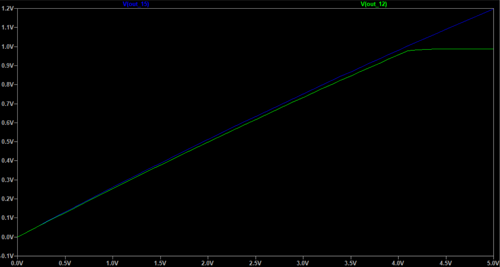
The output is also almost the same, with max output of the 12V being 0.98V instead of 1V:
I_abc for both 12 and 15V are exactly the same:
The voltages around the R_abc however, are very different as V_abc changes.
 |
| V_abc - these are fairly constant but drops abruptly when CV gets very small (the simulation used a resolution of 0.1mV, in reality the dropoff is even closer to 0VCV. |
By manually tweaking R_d I was able to get an exact match with unity gain for both voltages. The R_d for 15V is slightly lower than expected. Perhaps a different value than 0.7 for diode drop is used in the simulator?
Here are updated measurements.
CV inputs
| CV |
Supply |
Icv (=-I emm) |
I base |
Iabc |
Vabc |
V coll |
V base |
| 0V | 12V | 0V | 0V | 0A | -11.29 | -11.29V | 46.9nV |
| 0V | 15V | 0V | 0V | 0A | -14.27V | -14.27V | 46.9nV |
| 0.1V | 12V | -21.7uA | -224nA | -22.4uA | -10.47V | -10.28V | -675.9mV |
| 0.1V | 15V | -21.7uA | -224nA | -22.4uA | -13.47V | -13.28V | -675.9mV |
| 5V | 12V | -1.064mA | -10.5uA | -1.053mA | -10.26V | -1.62V | -775.6mV |
| 5V | 15V | -1.064mA | -14.3uA | -1.053mA | -13.26V | -4.63V | -775.6mV |
I've added an additional step at CV=0.1V, as the voltages around R_abc abruptly drop below this. This step shows that V_abc is fairly constant and not too far from the ideal supply-1.4V.
So, what can we see from this? The only thing that changes when we switch supply (after replacing with updated R_d) is V_abc (which in turn changes V_coll). I_abc vs gain stays the same.
They also stay the same even if I_d changes.
Signal voltages
- input is -5 to 5V.
- CV is 5V
- +in is connected to input through a 27k resistor and has a 510R to gnd
- bias input is connected to 12/15V through 12k/14.75k resistor
- Output is to gnd via 28.7k resistor, buffered.
| Supply |
+in |
-in |
bias |
I out (to gnd) |
V out |
| 12V |
175mV to 275mV
(191.7uA to -175uA in 27k, 343uA to 539uA in 510R, -535uA to -365uA into +in) |
184.5mV to 265mV
(373uA to 536uA) |
1.03 to 1.12V
(-914.5uA to -907uA) |
176.1uA to -174.8uA | V out: -5.05 to +5.02 |
| 15V | 183mV to 283mV
(191.9uA to -174.7uA in 27k, 358.5uA to 554.5uA in 510R, -550uA to -380uA into +in) |
191.9mV to 272.7mV
(391uA to 556uA) |
1.04 to 1.13V
(-946.8uA to -940.7uA) |
172.3 to -172.2uA | V out: -4.95 to +4.94 |
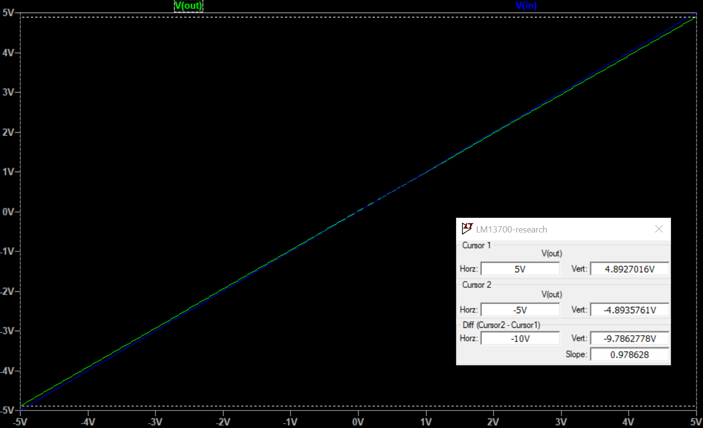
These are practically identical, I assume that a bit of tweaking for R_d would make them exactly the same. Nice! That means that the same I_abc gives the same gain as long as I_d is tweaked due to the changes in supply voltages.
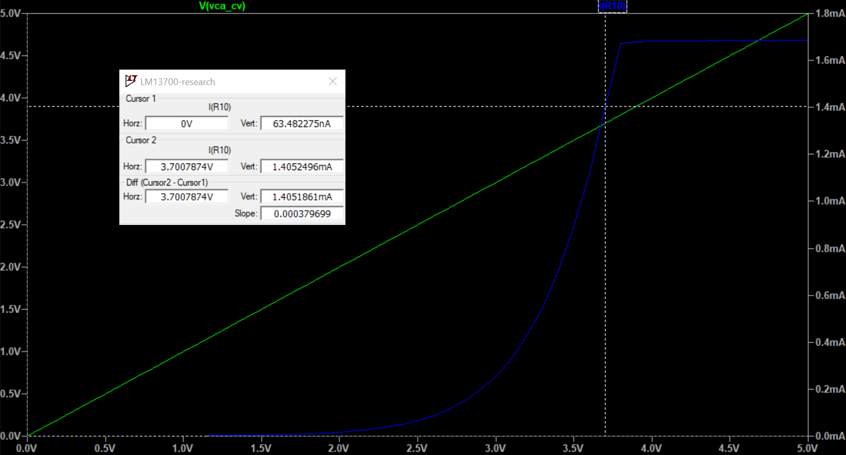
Juno expo converter
My juno expo converter is made to go to max, so it flatlines when CV > 3.5V. With adaptions between 12V and 15V (offset resistor and reference current resistor) they track the CV exactly the same, but the 15V version goes slightly higher.
 |
| 15V and 12V expo circuits (VCA linear control circuit is still present but not used) |
 |
| Both flatline when CV is high enough but 15V goes further |
Voltages around R_abc are different, as expected. I've reduced CV to 0-3.5V to stay within operating range
 |
| V_abc is still fairly constant, with about 0.5V variation |
 |
| V_coll |
Again, as long as I_abc stays the same, the output stays the same. The expo converter generates the same I_abc as long as reference current and offset voltages are adjusted (and we stay within a range where voltages around R_abc can change enough to generate I_abc).
But we can do more! If we replace the 8.2k R_abc with a 6.4k, we allow a larger current through it with the same voltage. Then we get the exact same range as with 15V!
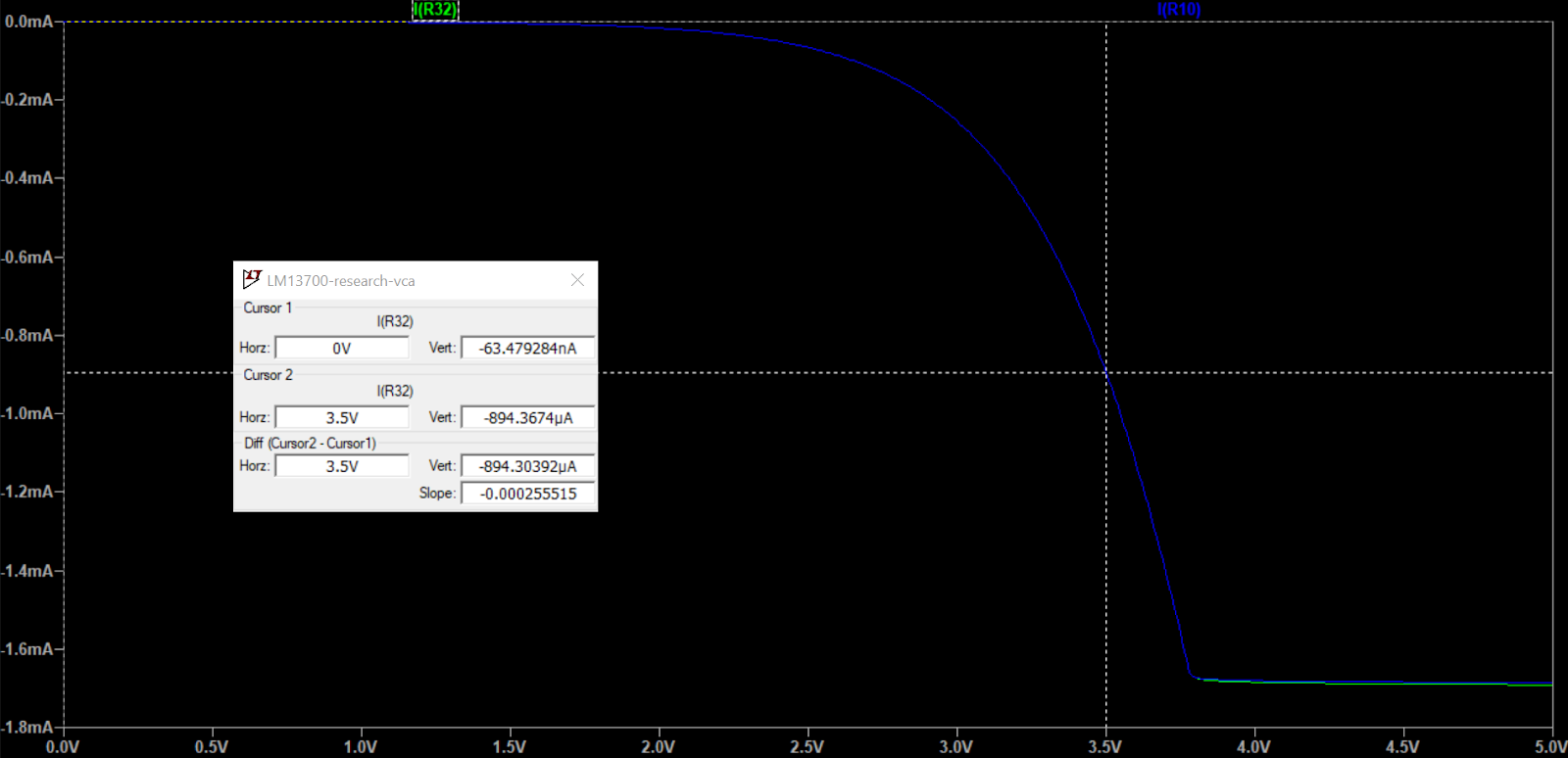 |
| I_abc are now equal for both 12V and 15V |
 |
| Outputs are equal too |
In other words, we could probably do the same for the VCA to get the same range there as well. Turns out, we can:
Xonik VCA again
Going back to the version from my failed post, which uses this circuit:
and has this output:
If we just replace the 8.2k R_abc resistor with 6.4k, it works as it should:
Gain without I_d
First, I tried a version of the circuit with and without I_d
 |
| Two versions of the 15V circuit, tuned to be approximately the same |
Signal input is -1 to +1V. From this plot it is quite clear that the one without I_d is not linear across the signal range:
 |
| The I_d version is completely linear whereas the non-I_d version is heavily distorted. |
Increasing the input resistor and thus get a smaller differential input gives us a much more linear result:
In the datasheet, gain without I_d looks like it is not depending on supply voltage at all. Here is a plot of a 15V and a 12V version:
 |
| 12V and 15V versions are very similar (but not 100%) |
I retried with a smaller input resistor, 30k. Here is the input and output voltages, you can juuust see that the output is not entirely linear:
 |
| Voltage at positive input |
 |
| Voltage at output, it is slightly curved downwards for the first 50% and then upwards for the rest. |
As is expected from the datasheet, when not using a diode biasing current, the input must be attenuated a lot more to keep the gain linear across the signal range.
Gain measured vs calculated
For the version without I_d
Gain is expected to be:
I_out = V_in * I_abc * q / 2kT
where
T = 283.15K (for 25C)
k = 1.38*10^-23 (Boltzmann constant)
q = 1.602*10^-19 (electron charge)
I_out = V_in * 19.47 * I_abc
(for T=300, gain is 19.3 * I_abc, which is almost exactly what is used in 8.3.3 and 8.3.4 in the datasheet).
This gives us for the 50k input version:
V_in+ is -11.18mV to 8.56mV, diff is 19.75mV
V_in- is -1.4959mV to -1.059mV, diff is 0,4369
V_in is -9.69mV to 9.62mV, diff is 19.31
I_abc = -1.05mA
Expected out is
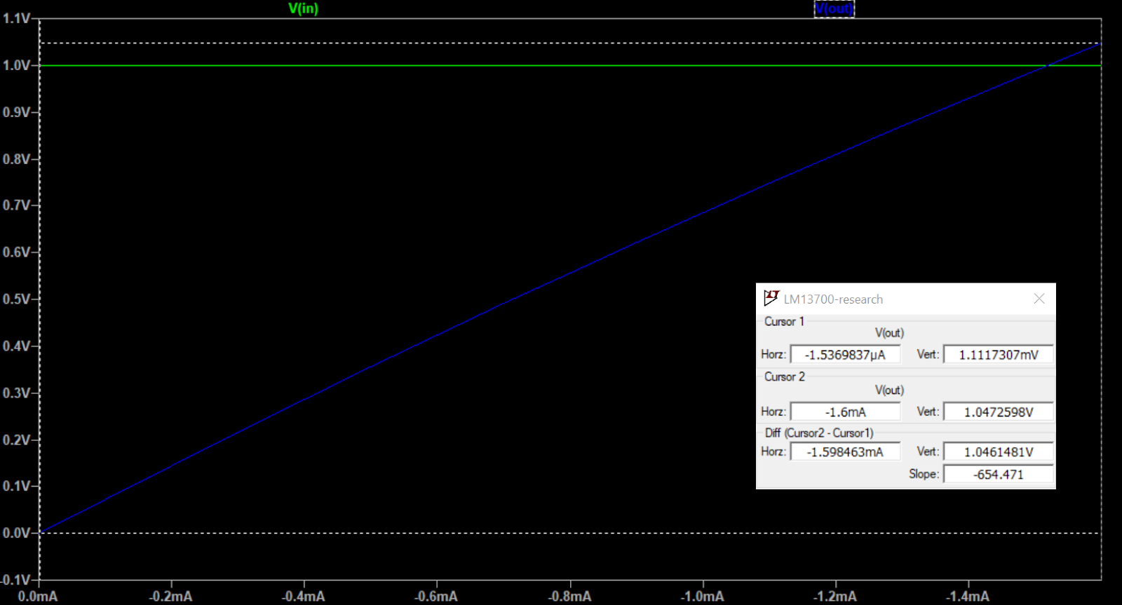
I_out = 0.01931V * 19.47 * 0.00105A = -392.3uA
Measured output current
I_out = 213.13uA -149.72uA, diff is -362.85uA
The output current is independent of the R_out resistor, it only sets the output voltage.
This is fairly close to what the gain formula predicted, which is good.
However, I still have NO clue as to how I can find V_in+, V_in- or the differential voltage V_in. Without the last one this formula seems useless.
The same goes for the "missing gain formula" for the version with I_d. It needs the current in the input resistor, but how do I get that when I don't know the voltage at V_in+?
Closer measurements and useful V_in
UPDATE: After doing the version with I_d, and the email from Iain described below, I did some further simulation of the circuit. This time with both input offset resistors to ground in place. (I think the results would be close even without the negative one, the output would just be less centered).
Since the formula for I_out depends on the differential voltage, we cannot assume that the whole voltage drop is across the input resistor.
However, the voltage at the negative terminal is much smaller the positive terminal, so we can choose to ignore it. We can also ignore the effect of the input transistor on the resistor divider formed by the input resistor and the resistor to ground. This means that an approximation of the differential voltage is
V_diff = V_in * R_g / (R_g + R_in)
where R_g is the resistor to ground.
When using the simulated differential voltage in the calculation, we get within 12-13% of the measured output value (for 500R resistors to gnd). Using the voltage divider voltage the error is 14-15%. I say that is plenty good enough :)
PS: The output current is not centered around 0A, this can be solved by either biasing or using a cap on the output.
 |
| 1V sinewave input vs current output. Output is not centered. Using R_in=200k and R_g=1000 |
 |
| Simulated and calculated results. |
PPS: The input voltages are not centered around 0V. To compensate for this, all voltage and current measurements in the spreadsheet above are the difference between the results for -1 and +1V input. Ideally, they should have been the averages, now they are twice that, which is why I've put 2x in all the columns. The formula still holds though.
 |
| With and without resistor from IN- to ground. Without (blue) the output has a larger DC component |
For the version with I_d
Now, I wanted to see how much off the "missing formula" was and how it worked with the simulated results, so I did a lot of measurements using 250, 500 and 1000R resistors to ground, and 12.5k, 25k, 50k and 100k input resistors. I also tried both 12V and 15V supplies but they turned out the same.
I also wrote Iain Sharp and asked how he calculated I_g. He very kindly answered me almost immediately (thanks again Iain!), and the main takeaway from his long and detailed answer was that since the input voltage drop is so large compared to the DC offset at the input, I_g can be approximated as V_in / R_in. Nice!
(In general, Iain Sharp confirmed my suspicion that no one really knows exactly how the LM13700 works and everyone just experiment to get the wanted results. Incidentally, he read the first part of this post and got very worried that I do such detailed simulations without actually breadboarding anything as simulations are not the real deal. I will definitely test stuff in real life).
Anyhow, here is a table that includes both the measured voltages and currents, the expected output voltage using the formula but with the measured I_g, and the expected output using the formula with I_g as V_in/R_in:
All measured numbers are the difference between the results of -1 and 1V inputs, as I have not AC coupled anything. This means everything is double, which is quite confusing I guess. But the results are still valid.
There are a lot of numbers here, but the most interesting are:
- For the "standard" 500R resistors, the error is around 16-17%.
- There is only about 0.5 to 3 percentage points difference between using the simulated I_g vs the V_in/R_in one. A bit worse for the 1000R resistors and better for 250R.
- The simulated I_g makes the error constant as long as the resistors to gnd don't change.
A better I_g
Now. I had a look at what V+ voltage to expect if using a resistor voltage divider and ignoring that the center is connected to a transistor and a diode.
Interestingly, the result is almost exactly twice what we get when measuring. If we wanted to get a slightly better approximation for I_g (and one with a consistent error as we change the input resistor), we could use
V+ = V_in * R_offs/(2*(R_in-R_offs))
I_g = (V_in - V+) / R_in
where R_offs is the resistor from V+ to ground.
We still have a bigger problem with the formula though, so it probably isn't worth it. Just find an approximate output and simulate/measure your way to the correct values!
The output in the version without I_d is not centered around 0, that is probably why there is a trimmer in the output VCA of the Juno filter, to add a DC component
Also, perhaps the filter does not use linearising diodes on the VCA as that allows a soft distortion similar to the non-linearity described above when the filter is overdriven.
DC operating point
The voltage input (base of the transistor) is not at 0 when the input voltage is removed, in other words, the input voltage at that point is centered around something else. If you need to find this, Iain Sharp had a nice way of thinking about it:
If you remove the input, you have two equal circuits around the differential transistors.
In one leg, you have D1 and R1, in the other D2 and R2.
Assuming R1 = R2, I_d is split equally between the two legs. We can also choose to ignore I_base as it is much smaller than I_d.
To get to ground, I_d must pass through R3 and the parallel equivalent of R1 and R2. Since R1 = R2, R1 || R2 is simply R1 / 2.
The combined voltage drop across the resistors is V_supply+ minus one diode voltage drop (roughly 0.7V) across the diode*. That gives us the formula for I_d:
I_d = (V_supply+ - 0.7V) / (R3 + 0.5 * R1)
Since I_d = I_R1 + I_R2, and I_R1 = I_R2, I_R1 is simply 0.5 * I_d
We can now find the voltage at the transistor base:
V_b = R1 * I_R1 = 0.5 * R1 * I_d = R1 * (V_supply+ - 0.7V) / (2 * (R3 + 0.5 R1))
V_b = R1 * (Vsupply+ - 0.7V) / (2R3 + R1)
* For the voltage drop I've assumed that 'reordering' the resistors and diodes so that it's R3 -> R1 || R2 -> D[1,2] and then calculated the equivalent resistance. I think this is ok but not 100% sure of it).
 |
| Tested circuit, input is +/-1V sine wave |
 |
| Input at V_b, centered around 452mV |
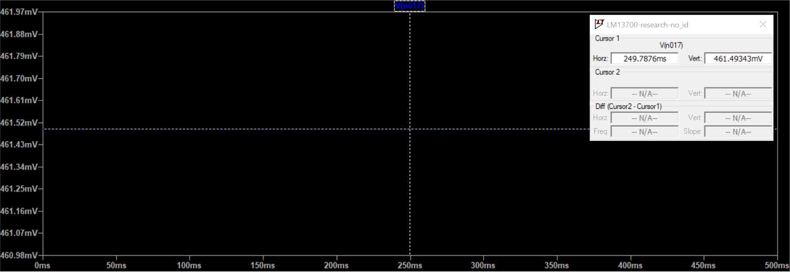 |
| Circuit with input and R25 removed, shows 462mV DC offset |
 |
Measurements and calculations - for all lines with a value (100k, 50k, 25k) the input was connected to gnd. For the "no input" lines, input and R25 was removed. V+ calc is within 0.01V of measured value
Value at start of header lines is R1,R2. |