Showing posts with label OTA. Show all posts

Friday, August 29, 2025

Adding overdrive to the ladder filter

If I need to add overdrive to the ladder filter, I can free up one CV channel already routed to the board by using the same CV for trimming 2 and 4 pole output. I just need to store the trimmer value for each and switch between then when switching mode.

Another thought is - the little phatty does not use trimmers on any of the OTAs, perhaps one can get away without them? 

Monday, March 20, 2023

A bit about how think about the basic operation of the LM13700

It's really hard to find any absolute truths about how to design for the LM13700 as the formulas available are not possible to use directly. Thus, most people end up simulating or experimenting until they get the desired results.

This post tries to give a few good starters for the most basic cases - using the LM13700 as a simple VCA without any feedback etc. Using the details here will get you in the ballpark of what you need, without being perfect. You then have to try various resistor values until you get what you need.

Maximum values from the datasheet

- I_abc: 2mA

- I_d: 2mA

- V_differential: +/-5V

Facts (of the not so fun type)

The relationship between I_abc and gain is independent of supply voltage, BUT:

  • I_d is directly proportional to supply voltage so the circuit generating it must be changed if changing supply voltage.
  • The voltage at the I_abc input changes with supply voltage, so HOW I_abc is generated changes if it does not come from an ideal constant current source.
  • Using the linearising diodes allows you to use a much higher input signal without distortion. A higher input means better signal-to-noise ratio, e.g. less noise on the output.

Design stuff

  • I_abc and I_signal should be as large as possible (for reduced noise), within the max/design limits.
    • When using the linearising diodes, I_signal can be much larger. 
  • I_abc goes through and sets up a voltage across R_abc. This has to follow Ohm's law, and so R_abc must be picked so that the voltage across can be large enough to hold up V = R* I for the I we want. It should not allow more than 2mA (I = V/R), any higher and the LM13700 self destructs. A bit of a safety margin is good, so maxing out at 1.8mA is fine. When switching from a 15V to 12V supply, R_abc must be reduced accordingly to allow the same I_abc range.
    • The voltage at the I_abc input is said to be two diode drops above the negative rail: V_abc = 2*V_be + V-. As a diode drop is approximately 0.7V, using a 15V supply we should expect a voltage of 1.4V -15V = -13.6V
    • In my simulations I've found this to be approximately true but it seems to change a little bit (around 0.5V) with control CV. It IS however consistent between 12 and 15V, with V_abc for 12V aways being 3V lower than for 15V.
  • When using the linearising diodes, gain is propotional to I_d.
    • Try to keep I_d = 1mA
    • I_d is calculated as (+V - 0.7V) / R_d, for example, for 15V supply and 13k R_d, I_d = 14.3V / 13kOhm
    • As I_d is not constant (it changes slightly with signal input), this will not always be the exact current, but it will give the correct relationship between I_d for 12 and 15V supplies
    • Keep | I_s | < I_d / 2  - I_s is signal input current, but it's not evident exactly what that means, see more about the missing/wrong formula for gain below
  • Differential input voltage must be < 60mV_pp (peak to peak) to keep THD < 0.1%. 
    • I am again not entirely sure what this means, but the datasheet uses an example with a 30k input resistor and a (trimable) 500R resistor to ground, and says that "the input divider in the input will reduce the 1Vp to 33mVpp. A simple resistor divider with 30k on top and 500R at the bottom will reduce a 2Vpp to 33mVpp so it may very well be just that, meaning that whatever input you have must be divided down so that it is at max 30Vp (single peak) or 60Vpp, ignoring any DC offset.
  • I don't understand how to select resistors to connect to +in and -in, but the norm is to use a 1k pot between the inputs with the center tied to GND. 
    • This makes it possible to trim out DC offset/CV bleedthrough from the output.
    • If the output coupled (AC coupling removes any DC component so any slight mismatch/off-centering will disappear)  two 510R to GND can be used instead.
  • Output current (and thus gain) when using linearising diodes can be approximated as I_o = I_g * I_abc / I_d
    • I_g is the current in the input resistor and is approximated as V_in / R_in
    • I_d is current into the diode biasing input and is (Vsupply - 0.7)  / R_d
    • The approximation is around 10-20% wrong
  • Output current when NOT using linearising diodes is I_out = V_in * q * I_abc / 2kT.
    • V_in is the differential voltage between the positive and negative inputs
    • k is the Boltzmann constant
    • q is the electron charge
    • k is the ambient temperature in Kelvin
    • q/kT = 38.7 V^-1 at 25C (yay, temperature dependence!)
    • A good approximation for V_in is to use the voltage at the resistor formed by R_in and R_g, the resistor from the input to ground: V_diff = V_in * R_g / (R_g + R_in)
    • The approximation is just 1-2 percentage points wrong compared to the simulated results, but the simulated results are 10-15% different than the calculated output. The real life results may be even more different.
    • The calculated current is for an AC-coupled output. In reality, the output has a DC component, meaning it is not centered. The resistors to ground lessens this effect. Adding a DC voltage to the input can also center the output.
  • Output current is converted to a voltage by sinking it to ground and buffering the output. The output voltage is then V_out = I_out * R_out

Changing supply voltages


The only part of the LM13700 that is really affected by changing the supply voltages, is the voltage level at the I_abc input, which is needed when selecting an appropriate R_abc:
  • The voltage at the I_abc input is said to be two diode drops above the negative rail: V_abc = 2*V_be + V-. As a diode drop is approximately 0.7V, using a 15V supply we should expect a voltage of 1.4V -15V = -13.6V
Other than that, the resistor that is used to generate the current into the linearising diodes, I_d, must be changed. 
  • I = (Vsupply+ - 0.7V) / R_d
Whatever circuit generates I_abc may need modifications. For the linear control voltage of the Xonik VCA nothing has to change. 

For an exponential converter, you need to change:
  • The reference current resistor to get the same reference current: I_ref = Vsupply- / R_ref
  • The offset voltage resistor is connected to Vsupply and must be recalculated
  • R_abc must be changed to allow a smaller (when going from 15V to 12V) resistor to pass the same I_abc
The currents and voltages around the inputs are independent of supply voltage, and the gain is proportional to I_abc with exactly the same ratio for 12 and 15V supplies. 

NB: All of this is based on studying the simulation results so a disclaimer is necessary, things may be a bit different in real life :-D

A bit of background


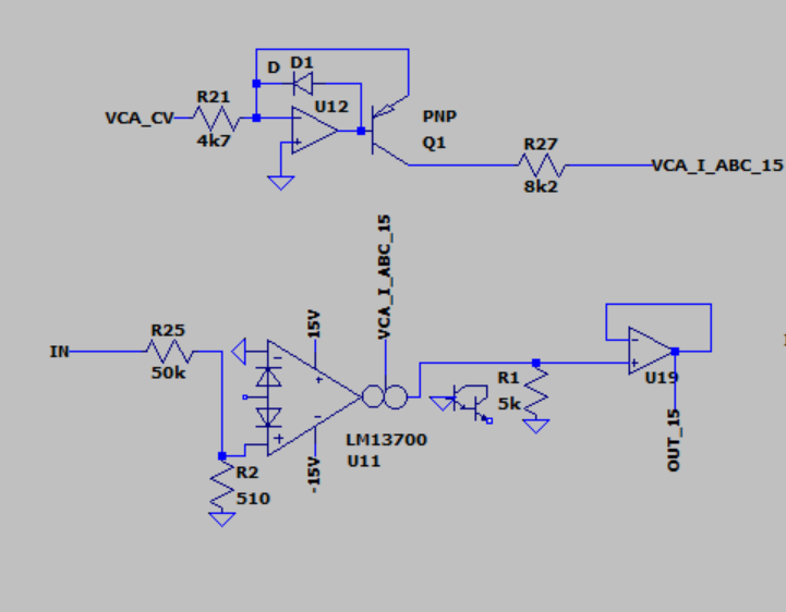
An example of the circuit using I_d / linearising diodes:


An example of the circuit without using linearising diodes. R4 may be replaced with a short but that will move the output more off center.


Formulas

Without an R_d/I_d:

- gain is said to be q * I_abc / 2kT. My simulations show that it is close to what the simulator says.

- kT/q = 26mV at 25C

- however, this is only an approximation for small differential input voltages. How small? Not sure, I can't find it even though I thought I read it in the datasheet.

- and you need the differential input voltage, but that can be approximated as described above.

With  R_d/I_d:

- gain is said to be I_out = I_s * (2*I_abc / I_d), for  | I_s | < I_d / 2

- however, nobody really knows what that means exactly, and what I_s is it seems.

- Iain from Lushprojects (http://lushprojects.com/blog/2012/08/lm13700-missing-forumla/) came up with an alternative formula: I_out = I_g * I_abc / I_d, where I_g is the current in the signal input resistor. It is said to be around 12% less than the actual gain but gives a ballpark at least.

- I_g can be approximated as V_in / R_in, in other words ignoring that the input is not at 0V. 

- The error in the formula is larger the smaller the biasing resistors get (and the smaller the input resistor gets), simply because the current in the biasing resistor increases relative to the input current. For the normal 500R biasing resistors, the error is around 17-19%.  

- The error in the formula are supply voltage independent.

The takeaway from these formulas are that the gain is dependent on I_d and that you can use a bigger input signal when using I_d, meaning less noise.

Links about the wrong formula: 

- http://lushprojects.com/blog/2012/08/lm13700-missing-forumla/

- https://modwiggler.com/forum/viewtopic.php?t=65783

- http://lushprojects.com/circuitjs/circuitjs.html?startCircuit=ota-gain.txt


A bit about the internals


Internally the circuit consists of four current mirrors and a differential transistor pair.

A current mirror is a circuit that makes sure that the current in two of its legs stays the same - one is the reference and one is the output - independent of what is connected to its output.

For this circuit, one of the mirrors makes sure the sum of the currents through the differential transistors, I_4 and I_5 here, equals the control current I_abc.

The three others bounces I4 and I5 around and combines them at the output, with the result being that I_4 + I_5 = I_abc

When trying to understand the circuit, it is useful to separate the analysis into two parts - what happens without any external AC input, and what happens with ONLY the AC input - as there will be a DC offset both at the input and output terminals.

Also, it helps to think about what voltages and currents are significant and what can be ignored/expected to be fairly equal.

Sunday, March 19, 2023

LM13700 12/15V simulations, second try

Before converting the JP6 filter to 12V, I wanted to know a bit more about what happens when changing the supply of the LM13700 from 15V to 12V. (For simplicity, throughout this text I will say 15V and 12V when I actually mean a +/-15V and +/-12V supply voltage).

As a first model I used the Xonik VCA.

Xonik VCA

I first calibrated the circuit for unity gain at 5VCV, 15V supply, then updated it for 12V by replacing the diode bias resistor and doing slight changes to centering. (Actually, I made the 12V first then calculated a new diode bias resistor by first finding I_d as 11.3V / 12k = 0.942mA, then finding a new resistor as 14.3k / 0.942mA = 15.18k. The voltage across the resistor is said to be one diode drop away from the supply voltage).


The output is also almost the same, with max output of the 12V being 0.98V instead of 1V:


I_abc for both 12 and 15V are exactly the same:


The voltages around the R_abc however, are very different as V_abc changes.


V_abc - these are fairly constant but drops abruptly when CV gets very small (the simulation used a resolution of 0.1mV, in reality the dropoff is even closer to 0VCV.


By manually tweaking R_d I was able to get an exact match with unity gain for both voltages. The R_d for 15V is slightly lower than expected. Perhaps a different value than 0.7 for diode drop is used in the simulator?


Here are updated measurements.

CV inputs

CV Supply Icv (=-I emm) I base Iabc Vabc V coll V base
0V12V0V0V0A-11.29-11.29V46.9nV
0V15V0V0V0A-14.27V-14.27V46.9nV
0.1V12V-21.7uA-224nA-22.4uA-10.47V-10.28V-675.9mV
0.1V15V-21.7uA-224nA-22.4uA-13.47V-13.28V-675.9mV
5V12V-1.064mA-10.5uA-1.053mA-10.26V-1.62V-775.6mV
5V15V-1.064mA-14.3uA-1.053mA-13.26V-4.63V-775.6mV

I've added an additional step at CV=0.1V, as the voltages around R_abc abruptly drop below this. This step shows that V_abc is fairly constant and not too far from the ideal supply-1.4V. 

So, what can we see from this? The only thing that changes when we switch supply (after replacing with updated R_d) is V_abc (which in turn changes V_coll). I_abc vs gain stays the same.

They also stay the same even if I_d changes.

Signal voltages

  • input is -5 to 5V.
  • CV is 5V
  • +in is connected to input through a 27k resistor and has a 510R to gnd
  • bias input is connected to 12/15V through 12k/14.75k resistor
  • Output is to gnd via 28.7k resistor, buffered.

Supply +in -in bias I out (to gnd) V out
12V 175mV to 275mV

(191.7uA to -175uA in 27k, 343uA to 539uA in 510R, -535uA to -365uA into +in)
184.5mV to 265mV

(373uA to 536uA)
1.03 to 1.12V

(-914.5uA to -907uA)
176.1uA to -174.8uAV out: -5.05 to +5.02
15V183mV to 283mV

(191.9uA to -174.7uA in 27k, 358.5uA to 554.5uA in 510R, -550uA to -380uA into +in)
191.9mV to 272.7mV
(391uA to 556uA)
1.04 to 1.13V

(-946.8uA to -940.7uA)
172.3 to -172.2uAV out: -4.95 to +4.94

These are practically identical, I assume that a bit of tweaking for R_d would make them exactly the same. Nice! That means that the same I_abc gives the same gain as long as I_d is tweaked due to the changes in supply voltages.

Juno expo converter

My juno expo converter is made to go to max, so it flatlines when CV > 3.5V. With adaptions between 12V and 15V (offset resistor and reference current resistor) they track the CV exactly the same, but the 15V version goes slightly higher.

15V and 12V expo circuits (VCA linear control circuit is still present but not used)

Both flatline when CV is high enough but 15V goes further


Voltages around R_abc are different, as expected. I've reduced CV to 0-3.5V to stay within operating range

V_abc is still fairly constant, with about 0.5V variation

V_coll

Again, as long as I_abc stays the same, the output stays the same. The expo converter generates the same I_abc as long as reference current and offset voltages are adjusted (and we stay within a range where voltages around R_abc can change enough to generate I_abc).

But we can do more! If we replace the 8.2k R_abc with a 6.4k, we allow a larger current through it with the same voltage. Then we get the exact same range as with 15V!
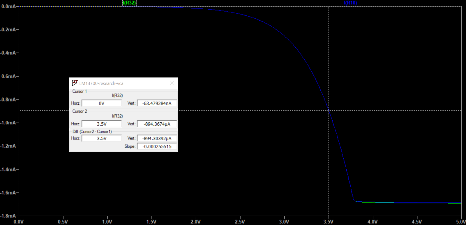

I_abc are now equal for both 12V and 15V

Outputs are equal too

In other words, we could probably do the same for the VCA to get the same range there as well. Turns out, we can:

Xonik VCA again


Going back to the version from my failed post, which uses this circuit:


and has this output:


If we just replace the 8.2k R_abc resistor with 6.4k, it works as it should:


Gain without I_d

First, I tried a version of the circuit with and without I_d
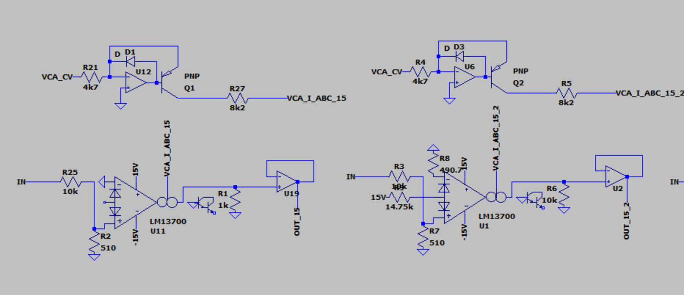

Two versions of the 15V circuit, tuned to be approximately the same

Signal input is -1 to +1V. From this plot it is quite clear that the one without I_d is not linear across the signal range:

The I_d version is completely linear whereas the non-I_d version is heavily distorted.


Increasing the input resistor and thus get a smaller differential input gives us a much more linear result:


In the datasheet, gain without I_d looks like it is not depending on supply voltage at all. Here is a plot of a 15V and a 12V version:

12V and 15V versions are very similar (but not 100%)

I retried with a smaller input resistor, 30k. Here is the input and output voltages, you can juuust see that the output is not entirely linear:

Voltage at positive input

Voltage at output, it is slightly curved downwards for the first 50% and then upwards for the rest.

As is expected from the datasheet, when not using a diode biasing current, the input must be attenuated a lot more to keep the gain linear across the signal range.


Gain measured vs calculated


For the version without I_d

Gain is expected to be:

I_out = V_in * I_abc * q / 2kT

where 

T = 283.15K (for 25C)
k = 1.38*10^-23 (Boltzmann constant)
q = 1.602*10^-19 (electron charge)

I_out = V_in * 19.47 * I_abc

(for T=300, gain is 19.3 * I_abc, which is almost exactly what is used in 8.3.3 and 8.3.4 in the datasheet).


This gives us for the 50k input version:

V_in+ is -11.18mV to 8.56mV, diff is 19.75mV
V_in- is -1.4959mV to -1.059mV, diff is 0,4369
V_in is -9.69mV to 9.62mV, diff is 19.31

I_abc = -1.05mA

Expected out is

I_out = 0.01931V * 19.47 * 0.00105A = -392.3uA


Measured output current

I_out = 213.13uA -149.72uA, diff is -362.85uA

The output current is independent of the R_out resistor, it only sets the output voltage.

This is fairly close to what the gain formula predicted, which is good.

However, I still have NO clue as to how I can find V_in+, V_in- or the differential voltage V_in. Without the last one this formula seems useless.

The same goes for the "missing gain formula" for the version with I_d. It needs the current in the input resistor, but how do I get that when I don't know the voltage at V_in+?

Closer measurements and useful V_in

UPDATE: After doing the version with I_d, and the email from Iain described below, I did some further simulation of the circuit. This time with both input offset resistors to ground in place. (I think the results would be close even without the negative one, the output would just be less centered).


Since the formula for I_out depends on the differential voltage, we cannot assume that the whole voltage drop is across the input resistor. 

However, the voltage at the negative terminal is much smaller the positive terminal, so we can choose to ignore it. We can also ignore the effect of the input transistor on the resistor divider formed by the input resistor and the resistor to ground. This means that an approximation of the differential voltage is

V_diff = V_in * R_g / (R_g + R_in)

where R_g is the resistor to ground.

When using the simulated differential voltage in the calculation, we get within 12-13% of the measured output value (for 500R resistors to gnd). Using the voltage divider voltage the error is 14-15%. I say that is plenty good enough :)

PS: The output current is not centered around 0A, this can be solved by either biasing or using a cap on the output.

1V sinewave input vs current output. Output is not centered. Using R_in=200k and R_g=1000


Simulated and calculated results.

PPS: The input voltages are not centered around 0V. To compensate for this, all voltage and current measurements in the spreadsheet above are the difference between the results for -1 and +1V input. Ideally, they should have been the averages, now they are twice that, which is why I've put 2x in all the columns. The formula still holds though.

With and without resistor from IN- to ground. Without (blue) the output has a larger DC component


For the version with I_d

Now, I wanted to see how much off the "missing formula" was and how it worked with the simulated results, so I did a lot of measurements using 250, 500 and 1000R resistors to ground, and 12.5k, 25k, 50k and 100k input resistors. I also tried both 12V and 15V supplies but they turned out the same.

I also wrote Iain Sharp and asked how he calculated I_g. He very kindly answered me almost immediately (thanks again Iain!), and the main takeaway from his long and detailed answer was that since the input voltage drop is so large compared to the DC offset at the input, I_g can be approximated as V_in / R_in. Nice!

(In general, Iain Sharp confirmed my suspicion that no one really knows exactly how the LM13700 works and everyone just experiment to get the wanted results. Incidentally, he read the first part of this post and got very worried that I do such detailed simulations without actually breadboarding anything as simulations are not the real deal. I will definitely test stuff in real life).

Anyhow, here is a table that includes both the measured voltages and currents, the expected output voltage using the formula but with the measured I_g, and the expected output using the formula with I_g as V_in/R_in:


All measured numbers are the difference between the results of -1 and 1V inputs, as I have not AC coupled anything. This means everything is double, which is quite confusing I guess. But the results are still valid.

There are a lot of numbers here, but the most interesting are:
- For the "standard" 500R resistors, the error is around 16-17%.
- There is only about 0.5 to 3 percentage points difference between using the simulated I_g vs the V_in/R_in one. A bit worse for the 1000R resistors and better for 250R.
- The simulated I_g makes the error constant as long as the resistors to gnd don't change.

A better I_g

Now. I had a look at what V+ voltage to expect if using a resistor voltage divider and ignoring that the center is connected to a transistor and a diode.

Interestingly, the result is almost exactly twice what we get when measuring. If we wanted to get a slightly better approximation for I_g (and one with a consistent error as we change the input resistor), we could use

V+ = V_in * R_offs/(2*(R_in-R_offs))

I_g = (V_in - V+) / R_in

where R_offs is the resistor from V+ to ground.

We still have a bigger problem with the formula though, so it probably isn't worth it. Just find an approximate output and simulate/measure your way to the correct values!

Other things to consider

The output in the version without I_d is not centered around 0, that is probably why there is a trimmer in the output VCA of the Juno filter, to add a DC component

Also, perhaps the filter does not use linearising diodes on the VCA as that allows a soft distortion similar to the non-linearity described above when the filter is overdriven.

DC operating point


The voltage input (base of the transistor) is not at 0 when the input voltage is removed, in other words, the input voltage at that point is centered around something else. If you need to find this, Iain Sharp had a nice way of thinking about it:


If you remove the input, you have two equal circuits around the differential transistors. 

In one leg, you have D1 and R1, in the other D2 and R2. 

Assuming R1 = R2, I_d is split equally between the two legs. We can also choose to ignore I_base as it is much smaller than I_d.

To get to ground, I_d must pass through R3 and the parallel equivalent of R1 and R2. Since R1 = R2, R1 || R2 is simply R1 / 2.

The combined voltage drop across the resistors is V_supply+ minus one diode voltage drop (roughly 0.7V) across the diode*. That gives us the formula for I_d:

I_d = (V_supply+ - 0.7V) / (R3 + 0.5 * R1)

Since I_d = I_R1 + I_R2, and I_R1 = I_R2, I_R1 is simply 0.5 * I_d

We can now find the voltage at the transistor base:

V_b = R1 * I_R1 = 0.5 * R1 * I_d = R1 * (V_supply+ - 0.7V) / (2 * (R3 + 0.5 R1)) 

V_b = R1 * (Vsupply+ - 0.7V) / (2R3 + R1)

* For the voltage drop I've assumed that 'reordering' the resistors and diodes so that it's R3 -> R1  || R2 -> D[1,2] and then calculated the equivalent resistance. I think this is ok but not 100% sure of it).


Tested circuit, input is +/-1V sine wave


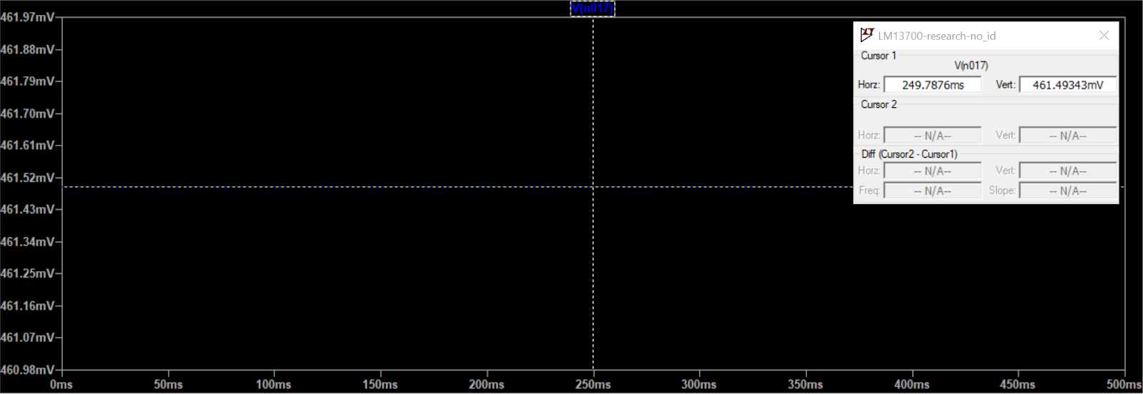
Input at V_b, centered around 452mV


Circuit with input and R25 removed, shows 462mV DC offset

Measurements and calculations - for all lines with a value (100k, 50k, 25k) the input was connected to gnd. For the "no input" lines, input and R25 was removed. V+ calc is within 0.01V of measured value

Value at start of header lines is R1,R2.


Thursday, April 9, 2020

Distortion breadboarded

I've breadboarded two versions of the distortion circuit, both with input attenuation and output amplification to keep a 10Vpp signal almost untouched.

Pre-distortion amplification


First I did the version with pre-distortion amplification. With distortion CV at 0V the distortion circuit sees around 30mVpp. This is heavily amplified to distort.

At the other end, a second OTA amplifies the signal. The output has unity gain for a 10Vpp input when CV is around 2.5V.


Hard clipping circuit with pre and post distortion VCAs

Hard clipping, distortion CV from 0 to 5V


Soft clipping circuit with pre and post distortion VCAs

Soft clipping, distortion CV from 0 to 5V


This circuit worked pretty much as in the simulation. I do have some issues with CV feedthrough so centering is not perfect when distortion changes.

I think I have to bite the bullet this time and introduce AC coupling to get rid of this. Placing a cap in series with the 1k resistor to the distortion op amps negative pole seems to do the trick, and will function as a high pass filter as well (beware though, if not chosen correctly low frequencies will not be distorted, in fact they will be attenutated.

Distortion CV at 0V

Distortion CV at 2.5V, almost full distortion and more than double amplitude

Distortion CV at 5V, full distortion. Signal is clipped unevenly by the op amp.

Distortion CV at 2.5V, almost full distortion


Distortion CV at 5V. Very similar to half distortion.

It seems that the real life circuit sees a higher maximum input gain than the simulation. Full distortion is reached much earlier. Also, compared to the OTA in feedback loop version below, the CV response seems exponential, not linear.

OTA and parallel resistor in feedback loop


Then I tried breadboarding the OTA-in-feedback version. I had lots of trouble and could not get it working as expected at all. After much experimentation I ended up with a well functioning circuit. I then started documenting the changes, and realised what was going on: I had inadvertently put a 33k resistor in the feedback of the distortion op amp. This works in tandem with the signal fed back through the OTA, so it completely changes the amount fed back.

As a bonus, the CV control of this version seems to feel much more linear - in the other version all changes came at the start of the CV and very little later. Also, the soft clipping amplitude seems to stay very close to 5V, so in some ways it feels more "correct", the volume doesn't increase as much.

After discovering my error I simulated this circuit too and it works as on the breadboard.

PS: The distortion CV now works in reverse: 0V is max distortion, 5V is no distortion. Unity gain through the circuit is the same as above, approximately 2.5V.

OTA and 33k resistor in feedback of op amp

Soft clipping

Hard clipping, starts very soon after turning the distortion pot.


OTA in feedback loop without the 33k resistor


Now I went back to the circuit that I was TRYING to breadboard and looked at the simulation again. I think I got lost because I couldn't get it working the way I wanted to. Looking at my previous Distortion post, I realised that the hard clipping starts much later, and so the output has a higher amplitude when clipped than in my happy accident.

I then changed parts back to my original design and did some tweaking, resulting in this circuit:


OTA and no resistor in feedback. Soft clipping version


OTA and no resistor in feedback. Hard clipping version
Soft clipping

Hard clipping

Results on the breadboard for versions with OTA in feedback loop


The circuit on the breadboard have some small differences from the simulated one. The output amp uses a 120k resistor instead of a 150k to get unity gain at 2.5V CV. I left the 180pF (Low pass filter) in place, and used 1k pots instead of the resistors to ground on the OTA inputs (except for the distortion OTA in the version without resistor in the feedback.

The potentiometer settings used were:
VCA pot: 620 ohm to ground on negative input, 365 ohm to ground on positive input
Distortion pot: 479 ohm to ground on negative input,  512 ohm to ground on positive input in distortion OTA. For the version without a feedback resistor I breadboarded it as in the schematics.


All oscilloscope pictures are of a 473Hz 10Vpp input wave. Vertical resolution is 5V/square. Output VCA CV is at 2.5V which according to the simulations should give us unity gain for undistorted signals.

First, the circuit with both an OTA and a 33k resistor in the feedback, soft clipping:


Triangle wave, soft clipping selected and distortion CV is at max (5V) meaning least amount of distortion. Output is equal to input
Same as above but with distortion CV at 0V, meaning max distortion. Amplitude only changes slightly but output is heavily distorted.


Hard clipping:

Same as above, but this time with hard clipping. 5V distortion CV, No signs of clipping and still unity gain.

Again same as above, hard clipping, but with 0V distortion CV/max distortion. Heavy clipping and just slightly higher amplitude.

Without 33k resistor in feedback

Now for the circuit without the 33k resistor in the feedback loop. This didn't work very well, the clipping became very asymmetrical. This may be due to the high attenuation of the input signal? I tried replacing the resistors at the positive and negative OTA terminals with a 1k resistor but that didn't change things. Maybe an HP filter capacitor would help?

Soft clipping:

Soft clipping, max distortion CV. The signal passes unclipped but with the output VCA CV at 2.5V the amplitude is only around 7Vpp, and also not symmetrical around 0V.

Soft clipping, no distortion CV. Heavy but unsymmetrical clipping. Amplitude is almost the same as for the previous circuit.
Hard clipping:

Hard clipping, max distortion CV. Same as soft clipping, no surprises there.

Hard clipping, no distortion CV/max clipping, looks very similar to hard clipping for the other circuit except that the clipping is unsymmetrical.


Pre and post OTA breadboarded


510 ohm resistors instead of trimmer for version with 33k in feeback

I tried replacing the 1k trimmer pot on the distortion feedback OTA with two 510 ohm resistors to ground. That gave the following result:


The input is now distorted, meaning the OTA sees a too high voltage.

By measuring the position of the trimmer potentiometer for the distortion feedback OTA when signal does not clip at 10Vpp input (750 ohm), and using the resistor divider equation, I found that the distortion OTA sees +/-165mV. Going the other way, a resistor divider with 15k and 510 ohm will yield the same result. Here I have done the change:


When tweaking the potentiometer I could see that clipping starts right after I started turning the potentiometer. Since there may be production differences, an even smaller input resistor would give a litte room for trimming the input digitally. Here is the effect of 12k, a slightly smaller amplitude:


I also tried replacing the trimmer in the VCA OTA part, that heavily offset the output. It could be possible to use AC coupling here, but we would still get uneven clipping in the VCA at high gain, so it might be best to use a trimmer.

I also did see a slight distortion at minimum distortion CV, but this is probably not related to clipping.

510 ohm resistors in the simulation

In simulations though, it does not work very well:

Signal is much smaller than in the breadboarded circuit when no distortion CV is applied.


I am not sure I will do any more work on this now, I have a well functioning circuit that I will test with some "real" signals instead later (the one with the extra 33k resistor in the feedback, 12k on the input and 120k on the output).