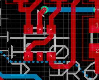
I have managed to mess things up with the JP6 filter as well. I've drawn one single trace using layer 97 - info instead of the trace, so the left base of the cutoff CV expo converter is not connected to GND.
This is possibly the single worst place on the whole board to err, as the transistor IC is soooo tiny:
Update 7th of July: I found a second error, R22 should be connected to the negative mixing point of the resonance OTA (IC4A), not the junction between R19 and R19 (pin 1 of IC2A).
After fixing this, and realising I had used a 100k instead of a 10k resistor between the VCA CV and the mixing point (resulting in a +/-0.5V swing instead of +/-5V), everything works beautifully.
However, the output of the first cell has a swing of +/-5V when +/-6V is expected. This can be fixed by increasing the output gain, but it means that the 100k pot on the output op amp is maxed out. One needs to increase the value to have room for adjustment (adding a 22k series resistor probably fixes it). Not sure why the cell output is too low, this must be investicaged further
Update 8th of July: I found a third error... The output is fed back into the wrong pin on the overdrive OTA, meaning it attenuates instead of overdriving the signal. I also forgot about a resistor on pin 15.
In a new revision I should also consider again if the overdrive should happen pre-output VCA, now it is not possible to keep volume the same when overdriving, output is almost doubled when max overdrive is turned on.


No comments:
Post a Comment