Wednesday, February 10, 2021

CV refresh rates

My Teensy-based voice controller prototype currently has a CV refresh rate of 1kHz. In this post I noted that the OB-6 has a refresh rate of 24kHz for < 1ms attack on envelopes, and the VS-1 OB-X remake uses 48kHz. I want my controller to get closer to those numbers.

I will have 48 CVs. Refreshing them at 40kHz means I need to update the DAC at 1.92MHz. With a 600MHz processor, this leaves around 300 clock cycles per update. It may be possible but could be a little on the short side.

I have tried dividing the CVs into those that will probably be modulated by envelopes, and those that can be a bit more slow moving. I ended up with 32 that I really want to be fast. If at the same time I reduce my refresh rate to what the OB-6 is using, 24kHz, I end up with a refresh rate of 768kHz for the 32 CVs. Add inn a 1kHz+ refresh rate for the remaining 16 and we end up with approximately 800kHz. 

In a new video on the VS-1 I noted that it now has 112CVs. It uses an 8 channel DAC, which means each channel has to be updated at 14 * 48kHz = 672kHz - that's pretty close to what I'm trying to do!


Necessary changes to my circuit

Capacitance

On the 1kHz version I use a 10nF sample & hold cap for 40kHz updates. Increasing to 800kHz means I should probably use a cap with 1/20 the capacitance. Closest match would be 470pF.

I tried putting this into my prototype but I'm having issues with noise - trying to generate a 800kHz square wave for testing doesn't seem to work very well. I switched to using my function generator but still had issues. It could be just because of the breadboard, so I will try this on a beta board, but before that I simulated the circuit in LTSpice to see what it looked like there. 


Initially I had a hard time getting the simulation to work. I couldn't get a proper square wave (I tried using the opamp comparator trick to turn my sine into a sqare), and started worrying that the TL072 is not up to the task. Perhaps the slew rate is too low? 

The datasheet says that the slew rate is between 13 and 20V/uS. In our case we want to charge the cap from 0 to 5V in  1/800000s = 5V/1.25uS = 4V/uS. So the slew rate should not be a problem.

After switching to the built-in pulse generator things looked a little better, but there were heavy noise on the square after I passed it through an op amp buffer. I then realised that by adding a resistor in series with the output, I would get a simple low pass filter. The formula for the filter is 1 / (2*pi*R*C). If we use a 470pF cap, and want an 800kHz cutoff, we need to use a 424 ohm resistor. A more standard value of 390 ohm gives us cutoff at 869kHz. Bear in mind though that this is a one pole filter, so the falloff is not very steep. Still, it should do away with some of the issue.

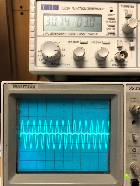
Simulating this turned out very well indeed, and adding it to the physical circuit also worked wonders for the INPUT to the S & H. The output, however, still looked the same. Connecting a 1k resistor between the output and the scope made it look a lot better.

Input vs output when using a filter resistor

Output still has some distortion at the bottom

Input, ringing is gone


I tried reducing the cap even further to get even higher refresh rates. This did not have the intended effect and I saw the same in the physical circuit as in the simulation. We get about the same response as with the 470pF cap. It looks like we're hitting some other limitation with the op amp perhaps - could it be internal capacitance or something? I'll see if I care to look closer into it.


Top: Square wave input vs output when we don't have a filtering resistor


Square wave vs unbuffered ("ideal") input to op amps (both top and middle are equal) and filtered version  (bottom) outputs


responses - top and middle are again equal and slightly rising towards higher frequencies, bottom shows low pass filtering,


Adding a similar passive filter to the output of the others - top and bottom show same response while middle gets a bit of a resonance peak.


Clock speed

The CD4520 clock can run at speeds up to 1.5MHz. I initially thought this too slow (for 1.92MHz, the refresh rate needed for 48 CVs at 40kHz it definitely is). I tried switching to a 74HC393, but running that at 3v3 meant the clock speed had to be around the same. The logic output also looked like 2V instead of 3v3,  and looked more noisy on the scope. Increasing Vdd to 5V let me run the chip at 3MHz and the logic output increased to 4V.

Something is definitely wrong here. Maybe it is the scope, maybe it is the breadboarding, but the 393 should be capable of clock speeds > 6MHz at 2V. I will test this further with my beta controller. It could also simply be that the timer I use cannot reach higher speeds than 2-3MHz. Oh well, it seems it may not be necessary after all.

As for the CD4051 mux, it probably has some of the same speed limitations as the CD4520. In the production version I will probably use vishay DG406 or similar which will probably work better.

Also, I may try to not use a clock at all, instead directly controlling the addresses of the muxes.


Addressing

To address 48 CVs I will either use 6 8ch MUXes or 3 16ch. Unfortunately, I cannot simply clock them sequentially. I can, however, use a clock for the three/four address lines, and then use the enable pin on each to select what mux to turn on. I would then update all 3/6 channels that have the same mux address sequentially to save time. 

I could possibly also use a separate mux to select which one of the other muxes to address. Doing this would actually make it possible to clock everything from the same clock (but possibly waste some clock cycles as I can either clock 4 or 8 muxes.


Multi channel DACs

Increasing the number of DAC channels would let us do less waits and also decrease the refresh rates since we would update multiple channels in parallel. This last thing is good as it lets us use a bigger cap that will keep its charge longer, giving us a more stable output.


Wednesday, January 27, 2021

Trying to create a CV curve to convert exponential VCA to linear.

In this post I'll try to explain exactly how the xxx2164 (SSM2164, v2164, AS2164 etc) responds to CV and how it (in theory) can be linearised when controlled digitally. I've written V2164 throughout the post as this is the chip I have at hand, but they should all be similar.

NB: I write my math as I go along, so it reflects my way of thinking. It may not be the most direct route to the final result, nor the best way of explaining, but at least I think the results are correct

Whether or not the results are useful in practice are to be seen. The V2164 is temperature sensitive and may not follow the stated -0.033V/dB response at all (or indeed any) temperature. There may also be differences between chips, and the DAC resolution may not be high enough to prevent stepping even when using 16bit DACs.

The V2164 

V2164 has a -33mV/dB response, meaning a 33mV increase leads to a 1dB attenuation.

When using the V2164 with a 3.3V control signal, I realised that it very quickly gets very quiet and thus it's hard to set the exact gain/ attenuation that you want. As mentioned here, the usefull CV range is 2V which results in 2V / 0.033V = 60dB attenuation.

The signal amplitude is doubled/halved for every 6dB change (0.2V in our case) as noted here. That would as far as I understand, mean that the signal is halved 10 times at 2V. With a +/-5V signal input, output would be

$$((((((((((5 / 2) / 2) / 2) / 2) / 2) / 2) / 2) / 2) / 2) / 2) = 5 / 2^{10} = +/- 0.0049V$$

But what is the function / relation between CV and VCA response?


Decibel - change in amplitude 

At any time, the increase in dB between two levels \(a_0\) and \(a\), can be written as

$$d = 20 \cdot log_{10}({a \over a_0})$$

where \(log_{10}\) is the 10-logarithm. From now on I'll write just \(log\)

For example, if the initial amplitude a_0 was 1V and the new level a was 2V, the increase would be

$$d = 20 \cdot log({2 \over 1}) = 6.02dB$$

which is indeed what we said above - a doubling of amplitude is the same as a 6dB change. Let's confirm this with our calculation above - going from 0.0049V to 5V:

$$d = 20 \cdot log({5 \over 0.0049}) = 60.2dB$$

So, how can we rewrite the formula to represent the relationship between our CV and output amplitude?

Let's first express the amplitude change as a function of change in dB

$$d = 20 \cdot log({a \over a_0})$$ $$10^{({d \over 20})} = 10^{log({a \over a_0})} = {a \over a_0}$$ $${a \over a_0} = 10^{({d \over 20})}$$

Taking it one step further to make it easy to plot, we move \(a_0\) to the other side:

$$a = a_0 \cdot 10^{({d \over 20})}$$


Let's check with our initial ratio:

$$a = 1 \cdot 10^{({6.02 \over 20})} = 2$$

Just as expected. Here is a plot of this function:

X is change in dB, Y is amplitude. We can see that the initial amplitude is 1 and that 6dB gives an amplitude of 2. Increasing dB by another 6dB to 12dB shows another doubling of amplitude to 4


From decibel formula to CV response

One final step is necessary, we need to go from the general equation for change in decibel to response to our CV. This should be fairly easy. We know that the response is -0.033V per dB (note: negative volt, i.e. a voltage increase leads to attenuation, not amplification):

$$d_{dB} = {v_{V} \over {-0.033_{V \over dB}}}$$

which gives us a as a function of v volts:

$$a = a_0 \cdot 10^{({{v \over {-0.033}} \over 20})}$$ $$a = a_0 \cdot 10^{({v \over {-0.66}})}$$


Let's check:

Increasing the CV with 0.033V should attenuate the signal 1dB, meaning that a 0.2V signal should attenuate the signal 6dB, which means halving the amplitude. We choose 1 as the initial amplitude, because with CV = 0 the V2164 should have unity gain. While at it, let's rename amplitude a to gain g as that is really what we're talking about when it comes to the VCA:

$$g = g_0 \cdot 10^{({v \over {-0.66}})}$$

\(g_0 = 1\) (unity gain when CV is 0) gives us

$$g = 10^{({v \over {-0.66}})}$$

and finally

$$g = 10^{({0.2 \over {-0.66}})} = 0.5$$

Again, as expected. Here is a plot of the function:

X is CV in volts, Y is gain (unitless). As expected, the signal starts at 1 when the CV is 0, and drops exponentially when the CV increases. at 0.2V the gain has halved to 0.5


Finding the equation for a linear response

Great! Now we know what we're up against. Next, we need something that takes a number - our internal linear control signal, let's call it c - and converts it into something we can input to the VCA CV to counter the function above. We need something that increases it's drop at the same rate as the function above decreases its drop.

So let's see what we've got.


We want the following to be true:

$$10^{({f(c) \over {-0.66}})} = k \cdot c$$

where k is a constant (rate of change, stigningstall in norwegian), in other words, we want something that makes our exponential function linear. We already know that \(f(c) = v\) from our definition, so let's use that.


Now we need to figure out what the relationship between v and c is:

$$log(10^{({v \over {-0.66}})}) = log( k \cdot c)$$ $${v \over {-0.66}} = log( k \cdot c)$$ $$v = -0.66 \cdot log( k \cdot c)$$

This works fine for positive k (e.g. rising linear response), which is what we usually want. However, after \(k \cdot c = 1\) it becomes a negative number which we cannot represent directly with a DAC. Also, when \(k \cdot c = 0\), \(log(k \cdot c)\) is infinite, which means we can never really reach all the way down to 0 gain using an exponentially controlled VCA.

As x approaches 0 from above, y approaches infinity. When x (or rather \(k \cdot c\) in our case) is > 1, y is negative.


Combining the equation for v with our equation for g yields exactly what we want - a linear response (rate of change k times control signal c on the horizontal axis, gain g on the vertical).


For a negative k (e.g. falling response), \(log(k \cdot c)\) is not defined for positive control signals c as \(k \cdot c\) is a negative number. To still be able to use a positive control signal c to represent a falling curve, we need to add something to offset our zero point: \(log(p + k \cdot c)\) where p is the desired gain at c = 0 (e.g. what we get when we set c to 0 and combine our two equations). 

The combined response is not defined for positive values of c when k is negative. 

Adding a constant "shifts" the graph to the right. Here p is 2 and k = -0.5: we get a gain of 2 when c is 0 and a gain of 0 when c is 4. NB: This is just in theory, as explained above we cannot reach g = 2 for c = 0 because the logarithm approaches infinity. More on that further down.


p may still be present for positive values of k, however the same limitation applies - if \(p + k \cdot c < 0\) the result is not defined, and if \(-0.66 \cdot log(p + k \cdot c)\) is negative it cannot be represented directly by a DAC.


Our relation between c and v is thus:

$$v = -0.66 \cdot log( p + k \cdot c)$$

with the limitations

$$p + k \cdot c >= 0$$ $$log(p + k \cdot c) < 0$$


Using this in our equation for the VCA gives us

$$g = 10^{({{-0.66 \cdot log( p + k \cdot c)} \over {-0.66}})}$$ $$g = p + k \cdot c$$

which is indeed a straight line with gain p at \(c = 0\) and gain 0 at \(k \cdot c = -p\)


How to use this in practice

Now, we still have the issue of not being able to reach g = 0. We need to look back at what we said in the beginning, the effective CV range of the V2164 is 0 to 2V, and at 2V it has an attenuation of 60dB (or gain of -60dB). This is what we should use as our minimum value for g. The maximum value should be whatever we want as our maximum gain, noting that unity gain (g=1) is the highest we can get using a DAC directly connected to the VCA.

We need to know exactly what we mean by -60dB in this case. Here, it means -60dB down from unity gain. A change in dB from an initial value of a_0 to a new value a is written as 

$$d = 20 \cdot log({a \over a_0})$$

For us, \(a_0\) is 1 so 

$$20 \cdot log(a) = -60$$ $$log(a) = -3$$ $$a = 10^{-3} = 0.001$$

Let \(c_{start}\) and \(c_{end}\) be the two extremes for our control signal:

This gives us two equations from \(g = p + k \cdot c\)

I) \(g_{start} = p + k \cdot c_{start}\)

II) \(g_{end} = p + k \cdot c_{end}\)

We can now pick our \(g_{start}\), \(g_{end}\), \(c_{start}\) and \(c_{end}\) to find k and p.

Let's give two examples based on whether we want a rising or falling response to our control signal. We choose to use volts as the unit for our control signal and set 0V to 5V as the range. We could also choose the range to match whatever representation we use in our code, for example 0 to 65535 if we represent the control signal as an unsigned int.


For rising control signals

\(g_{start} = 0.001\), \(g_{end} = 1\), \(c_{start} = 0V\) and \(c_{end} = 5V\)

I) \(0.001 = p + k \cdot 0 => p = 0.001\)

II) \(1 = p + k \cdot 5V\)

I + II) \(k \cdot 5V = 1 - 0.001 => k = {0.999 \over 5}\)

Finally, we insert this into our formula for v, \(v = -0.66 \cdot log(p + k \cdot c)\)

\(v = -0.66 \cdot log(0.001 + {0.999 \over 5} \cdot c)\)

Our desired response. A 0 to 5V CV gives a gain of 0.001 to 1

For falling control signals:

\(g_{start} = 1\), \(g_{end} = 0.001\), \(c_{start} = 0V\) and \(c_{end} = 5V\)

I) \(1 = p + k \cdot 0 => p = 1\)

II) \(0.001 = p + k \cdot 5V\)

I + II) \(0.001 = 1 + k \cdot 5V => k \cdot 5V = 0.001 - 1 => k = \frac{-0.999}{5}\)


It should come as no surprise that k is indeed the negative version of the result for the rising control signal, the absolute value of the rate of change is the same for both.

Again we insert this into our formula for v, \(v = -0.66 \cdot log( p + k \cdot c)\)

$$v = -0.66 \cdot log( 1 + \frac{-0.999}{5} \cdot c)$$

Increased attenuation as CV increases. 5V CV gives a gain of 0.001

From CV seen at the VCA to signal that controls the DAC

We have one final step to make all this useful.

We have from the start assumed that whatever we are working with outputs voltages directly from our control signal, and that our \(c_{end}\) outputs exactly 2V. 

This of course is not true for a DAC. We can choose to use a DAC in two ways:

  1. We use a reference voltage of 2V. The max DAC value is then 2V
  2. We use a different reference voltage, say 5V, and use external circuitry to change this into our 2V.

In both cases, we need to know what DAC control signal results in 1V at the VCA control input

Ex: 

If we're using a 16bit DAC and a 2V reference, 1V is represented as 65536 / 2 - 1

If we're using a 16bit DAC and a 5V reference, 1V is represented as 65536 / 5 - 1


Let s be the DAC control signal, \(s_{1V}\) be the DAC control signal value that results in 1V at the VCA input, and v the output voltage seen at the VCA CV input. The relationship between v and d is then

$$v = \frac{d}{s_{1V}}$$


Entering this into our expression for v, \(v = -0.66 \cdot log( p + k \cdot c)\), gives us

$$\frac{s}{s_{1V}} = -0.66 \cdot log( p + k \cdot c)$$

$$s = -0.66 \cdot s_{1V} \cdot log( p + k \cdot c)$$

There is a possible pitfall to be aware of. How well the effort to linearise the VCA works in practice depends on the DAC resolution. The VCA attenuation increases rapidly in the beginning, a very small voltage change gives a huge attenuation. If the DAC resolution is not high enough, each step changes the voltage too much and we will get audible stepping for slow moving CVs.


Summary of useful results

The general equation to linearise the response of the V2164 is

$$s = -0.66 \cdot s_{1V} \cdot log( p + k \cdot c)$$

where 

  • \(s\) is the DAC control signal value, possibly an unsigned int for a 16bit DAC
  • \(s_{1V}\) is the DAC control signal value that gives 1V at the VCA input (e.g. 65536 / 5 - 1 with a 5v reference)
  • \(p\) is the desired VCA gain at c = 0
  • \(k\) is the rate of change (gain / control)
  • \(c\) is our internal control signal with a unit of our choosing
\(p\) and \(k\) are found by selecting min/max gain and min/max control signal values, and solving the following two equations with two unknowns:

I) \(g_{start} = p + k \cdot c_{start}\)

II) \(g_{end} = p + k \cdot c_{end}\)

In practice, gain can never reach 0. For a positive k, p must be > 0. For a negative k we need need to use a g_{end} > 0.

Remember

- k changes when we change between volts and int value for our internal control signal.

- c and s do not have to use the same units

- c is assumed to be positive in all calculations above, but it may very well be possible to use negative values here. I just haven't checked.

- low DAC resolution will lead to audible stepping


Further thoughts

If I remember correctly, the V2164 allows gain > 1 by using a negative CV.  Without actually trying, I would think that using the equations above would suffice for this as well. If you want to add 3dB of extra gain, just extend the desired attenuation down to -63dB and then add - 0.1V (3  * -0.033V) to the DAC output to shift everything 3dB up. I have not tested this though.

To linearise a different VCA with a different response, "just" replace -0.033V/dB in the initial equation for the CV response and the resulting linearising equation. The general cases are:

Let b be the CV response in volts per dB (-0.033V/dB for the V2164). We then get that:

gain as a function of CV is:

$$g = g_0 \cdot 10^{\frac{v}{b * 20}} $$

necessary linearising equation is

$$v = 20 \cdot b \cdot log( p + k \cdot c)$$

and the DAC control value for producing that v is

$$s = 20 \cdot b \cdot s_{1V} \cdot log( p + k \cdot c)$$


The end. Time to try this in real life!


Footnote: All graphs are made using https://www.desmos.com/calculator


Friday, January 22, 2021

Exponential VCA v2164 and CV response

A quick note on the effect of a linear CV on the V2164. I connected a pot between 3.3v and 0. When turning the pot, nothing is heard until the pot is 2/3 of the way to max (CV drops from 3.3 to 0 as the v2164 expects a reversed CV, 0 being max on/unity gain).

Measuring the CV at this point shows as expected, around 1.2V. This means that for the rest of the pot's travel, it has no audible effect. This further strengthens my belief in using linear VCAs for the XM8. Alternatively, one could use a 0 to 1.5v cv, but it will never fully turn off the VCA. 

I'm looking forward to testing the same with a CEM3360/AS3360


Update: This article says that the effective CV range is 2V, which is more like what I experienced:

http://www.sdiy.org/philgallo/mgbvca.html

SPI error handling on the PIC16F

Various stuff happens in the SPI module that indicate errors. Here is a short description of what is going on.

Double buffering

SPI on the PIC16F uses a double buffer consisting of SSPxSR and SSPxBUF. 

SSPxSR is the shift register directly connected to the input, it receives bits when the clock runs. Once 8 bytes have been received, it transfers its content to SSPxBUF, sets the SSPxSTAT.BF (buffer full) bit and raises the SSPxIF interrupt. The BF bit is cleared automatically when reading SSPxBUF.

Data to be transferred is written to SSPxBUF and shifted out either immediately (for master) or the next time the other device runs the clock (for slave).

The following two bits indicate errors in transmission:


SSPxCON1.WCOL

Write Collision. Is set if the user tries to write a new byte to SSPxBUF before the current one has been shifted out/transferred. The data written to SSPxBUF is ignored, and all future writes are also ignored until the WCOL is cleared by the user.


SSPxCON1.SSPOV

Receive overflow. Is set if a new byte is received before the old one is read. Only used when device is an SPI slave. Slave must read SPPxBUF even before transfers to prevent the setting of this bit. On overflow, the current byte in SSPxSR is lost. 

In my DCO I check this when SS is driven high, before copying received data to where the user program expects to find it.


SSPxCON3.BOEN

Buffer overwrite enable. If set to high, data is written to the SSPxBUF even if the current byte has not been read. The datasheet does not say explicitly that it does or does not set the SSPOV bit, but it can safely be ignored. BOEN is used if we want to chain SPI slaves as one long shift register - data written to the slave will automatically be transferred to the SSPxBUF and shifted out once the next byte is received, without being touched by the user code. This way, one can keep the slave select pin low, transfer any number of bytes corresponding to the number of slaves connected, and then raise the slave select pin once all data has been transferred.

This is NOT used for my DCO as it will receive three bytes for each slave before the SS is driven high and thus has its own logic for shifting data internally.


SS pin 

The slave select pin synchronises reception. When in use it will be held high until the master is ready to communicate. The master will lower the pin, then transfer data and finally rise it. Using the SS pin makes sure data does not become out of sync and allows multiple slaves on the same SPI bus.

When the SS pin is driven high, the SPI bit counter is reset to 0, even if less than 8 bits have been received, meaning we will never get out of sync as long as SS is used.


SPI Initialisation

I can't find it right now, but I read that SPI must be initialised only when the clock is in the idle state. It may be that this is just because if not we risk getting incomplete/corrupt data, but it still seems like a good practice.

The way I've achieved this in the DCO is to initialise the SPI when the SS pin goes high the first time. That means that the master can either drive the SS pin low and high again, or it will happen automatically if data is transferred (but the data transferred will be lost) if the slave has restarted for some reason, or starts after the master has sent its first byte. This may not be the solution for everyone but it is sufficient for me. A different option would be to use some other scheme where an additional pin on the slave signals its status as "ready to receive" or similar.

To be able to do this, I had to both set use of SS to true and map a pin as SS, and add an edge trigger interrupt to the same pin. The edge bit should be set to 1 (rising edge).

Another PS for the use of SPI: The TRIS bits for the pins in use must be set manually upon initialisation;

SDI (TRIS set = input)

SDO (TRIS cleared = output)

SS (TRIS set = input)

SCK (TRIS cleared = output for master and TRIS set = input for slave)

Any function not desired may be disabled by setting the opposite data direction/TRIS value.

Wednesday, January 20, 2021

+/-12v vs +/-15v in XM8

CEM3360 may run at +/-12V or +15/-5 to -9V. Because of this, I have to reconsider if I should run the XM8 on +/-12V or +/-15V. I have done a quick review of my modules to see if they are 12v compliant.

Of my modules, these will run fine on 12v

  • Bitcrusher
  • DCO. NB: Needs 3v3 reference voltage
  • Reconstruction filter
  • Distortion
  • Sample & Hold


These will have to be fixed

  • CEM3340
  • Moog filter
  • Ring mod - looks like it's doing some kind of biasing
  • Super saw
  • Wave shaper - may just add external reference
  • V2164 VCA - R9 must be 6k instead of 7.5k according to http://www.sdiy.org/philgallo/mgbvca.html


These are unknowns

  • Jupiter 6 and Juno filters - use +/-15V for trimming and for setting an absolute cutoff for CVs, rest seem ok
  • Noise - has 220k res to 15v at input, need to test
  • v2164 - MD goes to 15v, may be possible to use 12v.


More on CEM3360 and voltages:

https://synth-diy.org/pipermail/synth-diy/2019-April/171021.html

On 3360: https://kassu2000.blogspot.com/2019/03/dual-vca.html

Tuesday, January 19, 2021

Envelopes, VCAs and linear vs exponential

TL;DR: 

  • Use linear VCAs when controlling them digitally, even when controlling audio. That lets you generate whatever control slope you want in software.
  • The VCA response is always exponential, not logarithmic. The only time we're actually talking about something looking more like a logarithmic response is in classic "RC" envelopes where the attack part is more logarithmic. Logarithmic control signals are generally only used to linearise an exponential VCA.

The full text

Through testing the digital envelopes in combination with the v2164 VCA, I realised that all is not good. It was particularly hard to dial in the sustain level as it dropped so fast when turning the pot due to the exponential nature. This made me realise that I had to revisit the topic of envelopes to fully understand how it is done in practice.

My initial confusion stems from the fact that people keep saying that you should use exponential VCAs for audio because they more closely approximate the way our hearing works. While this may be true when using the VCA as a volume control alone, it isn't necessary true elsewhere in the synth.

There is a lot of confusion about the use of the terms log(arithmic) and exp(onential) in the synth world, both when talking about potentiometers, VCAs and envelopes. I'll not go into detail, but just conclude that the slope/response is almost always exponential, not logarithmic. The only time we're actually talking about something looking more like a logarithmic response is in classic "RC" envelopes where the attack part is more logarithmic, and even here it is just an exponential response turned "upside down" (charging a cap instead of uncharging it). Logarithmic control signals are generally only used to linearise the response of an exponential VCA.

Another thing that is repeated is that using an exponential envelope with a linear VCA is the same as using a linear envelope with an exponential VCA. That is almost true, but with an exponential envelope controlling a linear VCA, you get direct control of the sustain level whereas when a linear envelope controls an exponential VCA, we get the "mapped" version of the sustain level which is significantly lower than the control voltage - which may be what you want but I found it hard to actually get the necessary control.

There's another point to be made though. When people talk about exponential envelopes, I suspect they mean the classic ones that is the result of charging and discharging capacitors, "RC" response. Those have a rapid increase upwards at the start of the attack and a rapid decrease at the start of decay. Using a linear envelope with an exponential VCA would give you a slow attack. 

A better name for the stages in an "RC" response envelope seems to be concave upwards and concave downwards. This is not what you get with an exponential VCA controlled by a linear envelope. 

Top: A linear envelope. Middle: The effect of feeding the linear envelope above through an exponential VCA. Note that the attack slopes downward and that the sustain level is significantly lower than the linear input as an exponential VCA drops very fast in the beginning. An exponential envelope would have the same shape but you would of course control the sustain level directly. Bottom: "RC" response, the classic envelope shape you get from charging/discharging a capacitor.


A lot of other versions exists. When you dive into the realm of digitally generated envelopes you find stuff like the Alpha Juno multi stage envelopes where the slope changes on a per-stage basis.

Alpha Juno lets you set envelope by specifying Time and Level for each stage. Slope varies from stage to stage, sometimes being linear (1, 2) and sometimes exponential (3, 4). These envelopes are purely digital.


One question was still unanswered for me - with an exponential envelope, should one make it control an exponential or a linear VCA? I've concluded that it has to control a linear VCA. The issue with sustain level speaks clearly of this. You want the response of the envelope, not an exponential version of it - especially when doing digital envelopes as you can pretty much do whatever shape you like. Hopefully, the resolution of the CV is high enough to mimic exponential growth with a fairly good quality even at low volumes.


What VCA chip to use in the XM8

Having to use linear VCAs kind of sucks. I was hoping to use the v2164 quad VCA extensively because it offers four VCAs in a compact package and at a reasonable price. If envelopes should control linear VCAs, and if I want to be able to patch envelopes anywhere, I also need to use linear VCAs everywhere. My best option seems to be the AS3330, which is a dual lin/exp VCA costing almost twice that of the V2164 meaning I have to spend four times as much on VCAs. That in itself kind of suck, but it will also take twice the space on the PCB which REALLY sucks. 

I will give the V2164 a final try though. If I can generate a logarithmic control signal, the output response will be linear. There is a very standard circuit going around that does this by combining two 2164s, but that sort of defeats the purpose. I have to do it digitally. This may result in very low resolution for the higher volumes, we'll just have to see.

Update: AS3364 is a quad linear VCA, that may be a good option. Unfortunately it's +/- 12V, not 15. I've ordered 10 of them for testing. I also realised that I have both AS3330 and AS3360 chips that I can try if I want. The AS3364 seems to be a dual AS3360 but with the exponential inputs removed, the text and specs in the datasheet is almost identical. This is good as it makes it possible to replace the AS3364 (which is an Alpha Rpar specific chip) with two 3360s on an adapter board later, should one fail and no replacements be available.


Resources

https://www.muffwiggler.com/forum/viewtopic.php?t=217707

https://www.muffwiggler.com/forum/viewtopic.php?t=115675

https://www.gearslutz.com/board/electronic-music-instruments-and-electronic-music-production/984069-embarrassing-question-explain-alpha-junos-envelopes.html

https://musicianonamission.com/adsr/

https://www.muffwiggler.com/forum/viewtopic.php?t=102357

First test with envelopes

It's alive! Last night I did the first test with a DCO, envelope and VCA. It worked quite well, some "thud" sounds at the start of the envelope, and a big issue with the DCO pitch that I later tracked down to it ignoring the low 8 bits of the pitch int, but it does indeed play notes :-D 

Here is a video of the test: https://www.youtube.com/watch?v=0isvi7EzVX4

I have yet to figure out the exact pitch bug but I have to send six bytes instead of three and every 2nd byte is ignored. It may have been intentional and should be a fairly easy fix. Also, I should considering resetting SPI buffers etc on SS high.

I did run into some issues with high DCO update frequencies (>100 times per second) so that needs to be checked too.

The envelopes however, works a bit strange. I guess that exponential VCAs is the reason, I had to have a very high value for the sustain level to get any sound. I will study this closer.

Also, to speed things up in the CV department (now the CVs have a 1kHz refresh rate) I need to replace the clock and mux, here are some alternative clocks:

https://datasheet.lcsc.com/szlcsc/Texas-Instruments-TI-SN74HC4040DR_C6848.pdf

https://datasheet.lcsc.com/szlcsc/TOSHIBA-74VHC163FT_C150161.pdf

SN74HC393


Monday, January 11, 2021

DCOs and 3.3v

A quick note on the DCO and Vdd. 

The chosen flash memory runs at max 4.6V. The Teensy 4.0 is 3.3v and not 5v compliant. That means we should probably run the DCOs at 3.3v too. However, that means the DACs must run with a 3.3v reference voltage too, as Vref cannot exceed Vdd. Thus we have to recalculate the charge voltages and possibly change the integrator cap too, to still be able to make a 5v output wave.

Also, we need to add an external resistor in parallel with R7 to get the correct calibration voltage.

Thursday, January 7, 2021

Winbond W25Q128JVSQ memory

I bought a bunch of flash memory chips from JLCPCB last time I placed an order there, to use with the DCOs and elsewhere where memory is needed. I chose the Winbond W25Q128JVSQ as it was quite cheap, part of the basic parts at JLCPCB and 128Mbit/16MB which should be plenty for the DCOs.

I thought it would be fairly easy to integrate with but boy was I wrong! :-D I've spent so much time now getting it to work properly. First I couldn't figure out how to write to it, then I got all wrong values back. I spent several evenings debugging this little bugger but FINALLY it works.

I will connect the chip to the same SPI bus as the DAC on the DCO, so it's important that it works with the same SPI mode as the DAC8830. Fortunately this seems to be the case, it works in both SPI mode 0 and 3. Both these have stable data on the rising edge of the clock, mode 0 has a clock idle low and mode 3 has clock idle high. The DAC8830 seems to work with mode 0 so I think I'll be fine.

So what did go wrong?

I'll explain the last thing first - reading back data. I managed to write data, but whenever I had multiple 1s followed by a zero, I'd lose at least one 1, and the missing bytes would be padded with 1s at the end! I wrote 0xAA (0b10101010), but reading it back it was always 0x87 (0b100001111). The first bit seemed to be correct at all times though. I checked 10-15 different values and the pattern seemed to be stable.

I did everything I could think of - writing to different memory locations, replacing the flash chip, slowing down the SPI bus - I even considered testing the memory with a separate PIC16F18346 (e.g. without the DAC on the SPI bus) but couldn't find any in my office (I'm testing from the DCO board).

Finally I tried adding a decoupling cap to the 3v3 input of the flash chip and it immediately worked! Turning the SPI bus speed back up to 8MHz also worked fine (on a side note, 8MHz SPI sampled at 24MSamples/sec on the Saleae Logic 8 does not seem to be fast enough to read it properly.

I'm so happy but also a bit mad at myself for neglecting to do this from the start.


So, what else. First of all, the JVSQ version of the chip is a bit special - it starts up in a different mode than usual but I don't think I ended up doing anything about that (or if I did it got persisted the first time, I need to recheck that. Also, the chip has two pins - pin 3 (HOLD) and pin 7 (WP). They are not needed in normal operation. I've tried both leaving them floating and connecting them to 3v3, both cases seem to work fine. The audio board for the Teensy has them both wired to 3v3 so I guess that's the safer option:

NB! Add a 100nF cap between pin 8 and GND for decoupling. When using with the DCO board, connect MISO/MOSI and SCLK to the DAC SPI bus pins, and CS to one of the UTIL pins

The CS pin needs to track the power supply pin on startup, so a pull-up resistor from CS to 3v3 is necessary.


Now to the procedure for writing and reading.

First of all, this being flash memory it has to be erased before it can be written. writing can only change values from 1 to 0, so erasing sets all bits to 1. 

To be able to erase, we must first remove the write protection - every time. This is done by sending 0x06 (as a separate command, pull CS low and return it to high before continuing.

Then send 0x20 (Sector erase, erases 4k bytes. Larger erases are also available) followed by three address bytes that should hit a 4k boundary.

After doing this we need to wait for the operation to complete before doing anything else. This is checked by sending 0x05, and then reading the result of status register 1 (in a loop) until bit 0 is 1.


Writing works the same way. First remove the write protection (0x06). Then send 0x02, followed by three address bytes, followed by 1 to 256 data bytes. NB: Writing wraps to a 256 byte page, so if you don't start at the page start but write 256 bytes, you will start writing from the page start once the end is reached.

After completion, we once again have to wait for the correct status, just as with erase.


Now we're ready to read. Reading is easy, just write 0x03 followed by three address bytes, then read the bytes you want.


SPI

I was confused by the various SPI modes. First of all, the datasheet for the PIC16F18346 says that data is written transmitted on idle to active or active to idle. It took a long time before I understood that this is in fact when the data CHANGES, not when it should be read. Transmit on idle to active means READ on active to idle.

To make matters worse, the text in the winbond flash datasheet (https://www.winbond.com/resource-files/w25q128jv%20revf%2003272018%20plus.pdf) says "The DO output pin is used to read data or status from the device on the falling edge of CLK". That is NOT SPI mode 0 or 3. Fortunately, the example timing diagrams show that the data is in fact to be read on the rising clock edge as is expected for SPI mode 0 and 3.

To top it all, the values of the two params of SPI mode (CPOL - clock polarity and CPHA - clock phase) are not consistent between different producers or places of documentation. Looking at these two, notice that the CPHA values for mode 2 and 3 don't match:

https://en.wikipedia.org/wiki/Serial_Peripheral_Interface

https://www.analog.com/en/analog-dialogue/articles/introduction-to-spi-interface.html#

The actual edges used matches though, so it's just a case of using different values for settings. Very confusing.

Monday, December 21, 2020

DCO 1.4 with memory / 3.3v Vcc

I intend to access memory from the DAC when using it as a wavetable oscillator. I have bought a large number of Winbond W25Q128 128Mbit SPI flash memory chips, however, they are 3.3v max.

That's not really a problem though - the PIC16F18346 and the DAC8830 runs fine on 3.3v, I just need to remember that when adding memory! I've tested and it looks ok. I can however NOT use 5v for the DAC reference, so to get the same output amplitude we need to recalculate the charge voltages.

DCO 1.4 tiny but major bug

Crap. I really messed up when I ordered the DCOs. I misread the datasheet, it says the DAC can drive loads of 60k unbuffered. I read this as "max 60k resistors" on the output, when in fact it is the opposite, minimum 60k. 

I even changed the 100k input resistor to 22k to prevent issues - 100k would have worked just fine :-(

I have tested the circuit and the effect is that the DAC is not able to get the output all the way up to 5V, it tops out around 4V and more importantly, at an unknown voltage. For charging the cap this may not be a big deal as the charge time is calibrated anyway, but for using the DAC as a wavetable DCO this really messes up things.

So, what can be done about it? Well, we have a few options

- 1: Replace R5 and R3 with 120k resistors (this lets us do what was originally planned, having a second external buffer to use as wavetable output.

- 2: Remove R3, R5 and R1 and R5. Replace R3 with a solder blob, effectively making an op amp buffer connected to ground, the same way we normally disable opamps. Then use an external opamp instead of IC3B, tapping the CHARGE_VOLTAGE pin and re-injecting the result at the CAP output pin. We may even be able to leave R3 in place, though I'll need to read up on this first.

- 3: remove R5 only, tapping the CHARGE_VOLTAGE, buffer it and then reinjecting at the other end of R5, however, that point is not exposed so we need a wire.

- 4: Desolder R5, cut the power lines and both cap inputs to the IC3 TL072 and use a whole separate one for both A and B.

Seeing as I can't solder anymore, option 2 or 4 is the simplest work for someone else desoldering the resistors, or me cutting the resistors in two. Option 2 will use a little bit more power as the opamp will still be in place, option 4 requires more opamps on the "main" board.

Distortion tested

 I breadboarded the distortion PCB today and it works as it should. 

As designed the overdrive is effective from above 5v, and tops out at approx 10V for soft clipping and a bit higher for hard. This means that the output is a lot louder when distorted, but that can be adjusted using the gain pot.

Take these considerations when wiring on the breadboard:

- If no filter caps are used, you must put a wire between the two HP pins (3 and 4). 

- Use a 200/100k resistor divider from 15v to a positive input opamp buffer to get 5V for the logic level

- Use a 10k resistor to GND on the clip mode pin, then you can use a wire from clip mode to 5v to change mode without removing the GND connection

- Input/output: I used my i/o module. Input should be amplified 5x (2x att, 10x gain), output should be attenuated 5x (10x att, 2x gain). Even with this, the input is not high enough to distort. I had to add an additional inverting amp (10k input and 100k feedback resistors, 10x gain) to get proper distortion.

PS: I have a couple of errors on the I/O board: the 1/4" jacks have Tip and Ring swapped so it shorts when using a mono cable. Also, the silk screen is wrong, it says that Gain is 2x when jumper is open and 10x when closed, it should be the other way around. Also, it seems that there is a fair bit of HF loss but that may have been before I got att/gain set correctly.

Sunday, December 20, 2020

Muliplexed evelopes

I've dreaded doing the envelopes for a long time, mostly because there is always something crazy happening that takes a long time to debug. But now I have a very good working prototype.

I looked at my previous post here: http://atosynth.blogspot.com/2015/02/sample-and-hold-acquisition-time.html

Using 10nF sample and hold caps I wrote (5 years ago...) that an update time of 25uF seems appropriate. I have, however, not shown the original circuit, I have to go back and check if I buffered the op amp or not - because when I redid it now I could not get the desired speed. I had to run updates for at least 50uS. When I added an opamp after the dac however, things changed. I can't see any difference even when I run updates at 16uS. 

So, I've written an arduino program that updates a dac every 25uS. This is multiplexed to as many channels as possible, and the overall refresh rate is 1kHz.  I had a lot of issues related to starting/stopping the various times and ended up with a 25uS timer running all the time, just turning off the DAC update when all channels have been updated.

The output chain goes like this:

DAC8830 -> TL07x buffer -> CD4051 mux -> output buffer, 10nF cap + TL07x 

The mux is controlled by aCD4520 clock (only two pins needed for clock, one for next and one for reset-to-zero). Before an update, the inhibit signal of the mux is raised, turning off the outputs. The clock is progressed, switching to the next output. The DAC is updated and settles in 1uS, then inhibit is turned off and the output turned on. It is left to charge the cap for the remainder of the time between DAC updates, approximately 16uS. Rinse and repeat.

I tried updating a square wave at 1kHz too, it looks surprisingly good. The edges are slightly rounded, but that seems to be an artefact of the caps as increasing the charge time does not affect it.

DAC control. 1: chip select, 2: SPI clock. 3: DAC data, 4: mux inhibit

1kHz square wave on one of the outputs

Envelope output, 1kHz sample rate

Closeup of steps. Each step is held by the sample and hold cap, the DAC is disconnected right after the start of each step


Friday, December 4, 2020

Tons of new circuits ready!

So much has happened this summer and fall, and I haven't written about half of it! Some of it is directly related to the XM8, but most is utility circuits. I simply decided that I had to take time to do do some intermediate steps before building the final voice cards.

A shortlist of circuits I've designed, breadboarded, tested and finally produced at JLCPCB/DirtyPCBs follows below. Everything has been soldered by my good friend and colleague Stig-Rune!

Analog CV bank with 16 CVs in groups of 4.


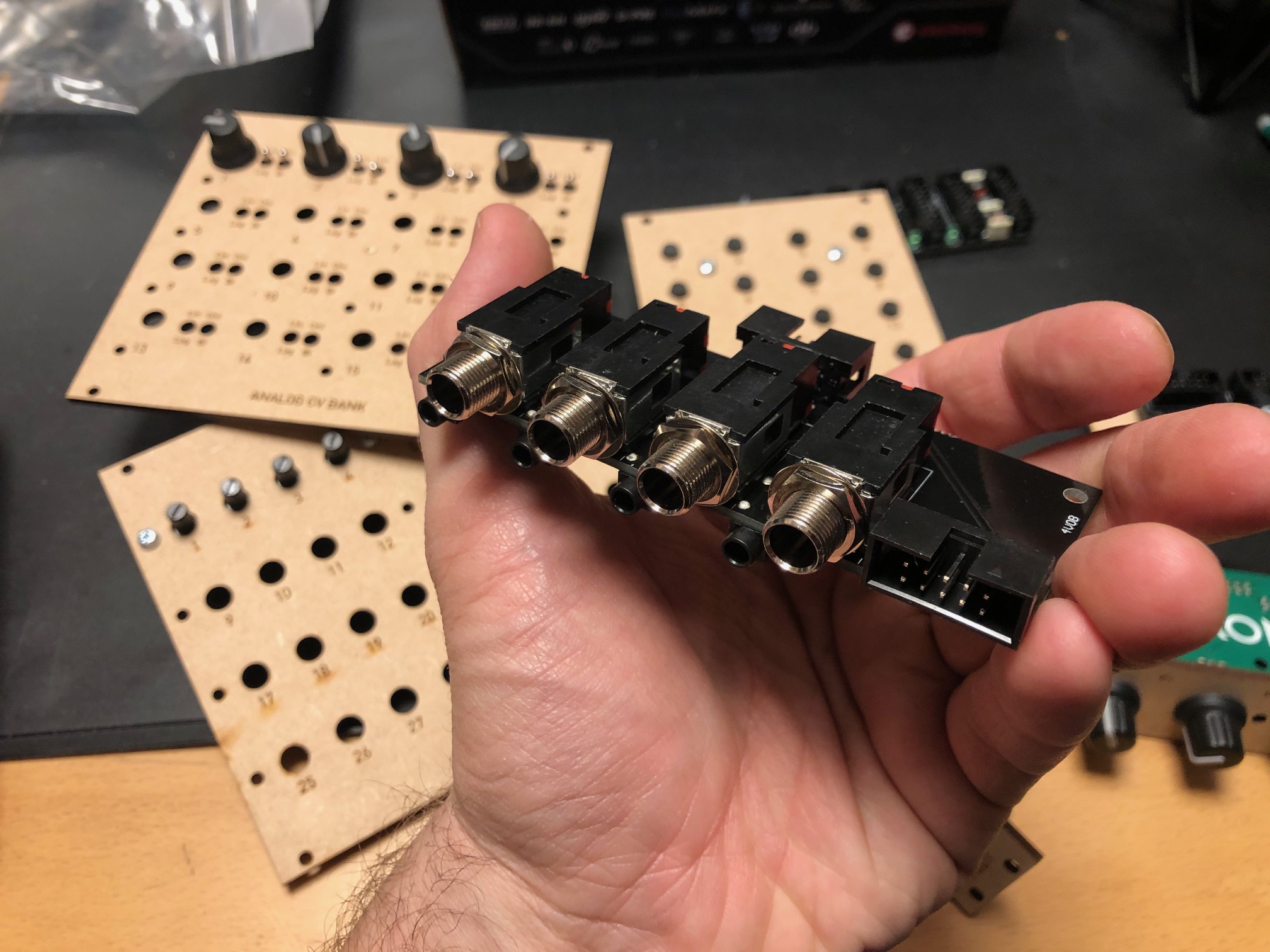
For each CV you can select between lin or log/antilog  response, as well as uni or bipolar operation. Per group of four you can select the CV range, 0 to 2.5V, 5V or 10V (or +/-2.5V etc for bipolar). I did fuck up the PCB slightly so I had to cut a trace in three places and solder a wire. Also, I messed up a cable so I shorted the outputs, almost overheating the opamps. After that it worked perfectly. Output is via 10 minijacks and a 10p IDC connector for easy connection to a breadboard.


Quad input/output module with 1/4" jacks


For each module you can select input or output connected to the 1/4" jack, and the opposite will be connected to a minijack. Both ends are also connected to a 10p IDC connector for easy connection to a breadboard. For each channel there is an option of 10 or 2 x attenuation and 10 or 2 x gain, meaning you can either have a unity gain circuit, a 5x attenuation (for line out-ish) or 5x gain (for input).


24/48 button module, digital

A digitally scanned button module (without the microcontroller), chainable for up to 48 buttons. Serially read so it only requires four pins + power, making it possible to combine it with the potentiometer module on the same cable.


8 to 64 potentiometers module, digital


A digitally scanned potentiometer module (without the microcontroller). Each module has 8 potentiometers, and 8 modules may be chained for a total of 64 potentiometers. As with the button board, it only requires four pins, and it shares the same clock and reset pins at the button module so a total of six pins + power is needed for all digital modules. During testing I discovered that pin 9 on IC2 - one of the address lines - should have been connected to GND. Now it is floating, so it isn't possible to set the address correctly. It's an easy fix however.


4 x IDC Passthrough module

A simple panel with IDC connectors on both sides, makes it possible to route IDC connectors as a group through the front or back panel without putting the cable through a hole.


Bitcrusher

A combined 12 bit sample rate reducer and bit rate reducer with analog and digital control, based on a PIC16F18446 microcontroller with built-in ADC. Described in separate posts. I've ordered 25 of these.


20kHz LPF

A filter module that can be used as an anti-aliasing filter for ADC input and reconstruction filter for DAC outputs. I use the same configuration in the Bitcrusher and intend to use this for the combined DCO/wavetable oscillators. The circuit comes from this page: https://www.analogfilters.com/anti-aliasing-filter/


Voltage Controlled Distortion

A distortion module for the XM8, the second of the two pre-filter FX (the bitcrusher being the other). Controllable distortion amount and output amplitude, as well as switch between hard and soft distortion. Untested.


Memory


A DIL mounted SMD chip, 128Mbit, for use as sample memory for the wavetable oscillators etc. Untested.


Prophet VS keyboard controller

A new revision of the 68b01 clone for the Prophet VS. I've ordered 20 of these so I have for future sales. They have all been programmed but are missing legs.


Modular synth power bus board

16p Doepfer standard boards with 7 connectors. A bit short but cheap to build.


10p and 16p breadboard IDC connectors

Tiny boards with an IDC connector on one side and legs on the other, making it easy to use ribbon cables between breadboards and modules


Unbuilt designs

In addition, I have PCBs for the following that has NOT been soldered yet:


Breadboard power and I/O module

Has input for +/-15v and a regulator for 5V. Also has IDC connectors for chaining multiple boards, and small chain-boards that can be fitted upside down to connect multiple boards. Connects to the power busses on the breadboard. No more risk of messing up polarities! Also: a 10p Doepfer compatible power connector, although the doepfer uses +/-12V, not 15V, and a 10p I/O connector that connects a ribbon cable to 10 pin headers for easy and stable connections. Pin 10 may be connected to ground with a jumper.


Breadboard coax connector and I/O module

A board with four coax connectors and the same 10p I/O connector as the board above. Will give stable connection points for oscilloscop, function generator and other gear that uses coax.


15-to-12v DC converter module

A module that converts +/-15v from either a molex connector or a 10p IDC connector to +/-12v and +5v. Output is through a 16p connector, compatible with the Doepfer standard. Also has a two pin header for injection of Gate and CV 


All in all 16 different boards! Needless to say, I'm more than pleased! I'm getting so close to being able to test an initial voice board, I just need to program some digital envelopes.


Bonus

I finally got the following soldered and ready for testing:

Two versions of the sample and hold buffer, one with some large caps and some filtering and one in a tiny DIL14 format, both quad sample & hold:


Then the second version of the DCO, this time with DAC output to make it a wavetable oscillator too:


Saturday, November 21, 2020

Bitcrusher tested

I got the bitcrusher from JLCPCB working today. Last week I discovered that some of the tiny 0402 resistors had lifted from their pads, so the input filter did not let the signal through. Last night my wife soldered them (I love her and how skilled she is, those parts are soooo small!), and today I was finally able to test everything.

The left pad of the two 0402 resistors have lifted. Not sure if this happened in production or when the pins were soldered.


I am still surprised at how recognisable the output is at 1 bit 27kHz. It has a lot of noise, but the music is still very audible. I am still not entirely convinced that it does not leak from the input, but when I reduce to 0 bits everything goes silent so I guess it is actually possible,

I had a lot of trouble getting the sample rate high enough, currently the max is at 27kHz with a 1:1 prescaler on timer 1 and a timer start value of 0xFEFF. Changing to 0xF0FF drops sample rate to 2kHz, so it's really sensitive. I need to work more on this but I am fairly confident that 44kHz should be possible.

I still want to confirm that the filters work as expected and have a 20kHz cutoff, but if that works as expected I think I'm ready to mass produce the filter. Perhaps just doing a quick input SPI check first.


Here is my test setup btw, for future reference.


I've also tested the filter response for the input filter. It works fairly well although there are some slightly strange things going on. 

First of all, at 10-15kHz, the output signal (what the ADC sees) is amplified slightly, before it drops towards 20kHz. At 20kHz it is close to what I see in the simulation, so that's great. At 25kHhz it is even lower than what was simulated. There is also some distortion on the sine wave, not much but visible. I'm not too worried though, as this is not a hifi system. The tests sounded good enough to me. I'm more worried about the phase shift I see even at low frequencies, They may be very audible if the signal is mixed with the original. We'll just have to see (hear).

5kHz - no amplitude difference but a slight phase change

10kHz, the output has suddenly increased by 0.2V (5-10%)


At 20kHz we have a very visible attenuation. The filter is designet for 20kHz cutoff

Heavy attenuation at 30kHz


Friday, November 6, 2020

Shanpu switches

 I got a shipment of sample switches from Shanpu in Taipei today. I had to pay full DHL express freight but they were very nice and sent me the samples for free. I will be able to buy directly from them in multiples of 100 of each item, and the price ends up at around $1.4 per switch including cap, but shipping and a rather steep low-volume fee of $100 for orders below 1000 means the real cost is closer to $3-4 depending on the number of switches I buy.

There are several switches to choose from. All are rated at 1,000,000 cycles!

The SPH2S has an audible click and a short travel of 0.2 to 0.3mm, 190 +/- 50gf force

The SPH2T has a very audible click and a medium long travel of 0.4 to 0.6mm, 230 +/- 50gf

The SPH2N has a no audible click and a very long travel of 1.0 to 1.4mm, 60 +/- 40gf


Then there is a low profile version, but it is only rated for 100,000 cycles, so unless it is more suitable due to the low profile, I should really go for one of the others.

The SPFSP1 has an audible click and a short travel of 0.2 to 0.4mm, 200 +/- 50gf force


In some ways I like the N version best, it sits somewhere between the keyboard switch feel of the Nord keyboards and the normal clicky synth button. It doesn't feel quite right somehow though, it's like the travel is a bit too short or something.

The T is a bit too noisy for me, so that leaves me with the S. The click feel of the S is closest to the D50 when comparing to some of my synths. It is a little bit on the heavy side though, switching between it and the N makes me think I like the feel of the N better.


But then there is another issue - caps.

I ordered six different caps in four different designs

YCA085C, a 9.6mm round, transparent black cap with a "lense" effect on top. It turns out that it is glossy, and because of the way it has been made, with a hole in the center, the light is rather uneven. Not too much, but it is not the best.

YCA151A, same as YCA085C, but one mm shorter and Ice color (translucent white). The light is much better, but this may simply be because more light gets through due to the color, or it is because it is 1mm shorter. I have to retest the black one with a smaller diode. Of course, its white when switched off, so it will not blend into the design if I choose a black front panel.

YCA080C, an 8mm round transparent black cap. It has a more frosted look and is flat on top. It looks really great and the light is much better too. It has ONE major drawback though, and that is that it's only 3.3mm long. If I use a 3mm panel, or a long travel switch, it is simply too small for me. It's really a shame, because it's hands down the winner when it comes to looks. Oh, and it would be a perfect match for the 8mm black alu 

YCA059C, an oval transparent black. It is too small for my liking.

YCA044A, a square, 7.5mm ice white cap with a slightly rounded top. It looks good, but is too thin, and the led is clearly visible through, so I can't use it.

YCA043C, a square, 7.5mm transparent black cap with flat top. Unfortunately it is simply too transparent and completely useless. It WOULD however make a perfect base for glueing the black 8mm alu caps on top of, if I want to use them with the same switches. I may even use them for the red square Aliexpress caps.

Bonus test: The red square aliexpress caps look ok with the led, though they have an internal pattern that is very visible. It doesn't really look like they are meant to be backlit.

That means that I'm probably down to two options: The biggest round transparent black cap with whatever switch I like the best, or the 8mm round cap with the S-model switch and a thinner panel. I must test if I can get away with 2mm aluminum.


Update:

1 - There is an even better option for attaching aluminum caps: They sell a 5mm round cap, YCA052, which probably will fit very well inside the aluminum - perhaps with a 1mm gap that could possibly be filled with glue? There is also a 6mm one, YCA046. Perhaps I should buy both just to check. BTW: The top of the alu cap may be too thick for this option, but the extra cost of buying 100 caps is so little that it would be stupid not to do so.

2 - For the switches where the led will NOT be used, it would be possible to put a piece of black cardboard inside and coloring the edges of the cap holder black to get a much darker cap - the white parts shine through and making the insides black helped a lot.

3 - changing from a 270Ohm to a 150Ohm for the thicker transparent black cap helps. Still not as good as the other though, so I definitely have to test 2mm aluminum panels.