Showing posts with label Wavetable. Show all posts

Sunday, June 28, 2026

Wavetable oscillator

I need a more precise sine wave than I have at the moment, with a larger range than I can get from the DCO.

That gave me an excuse to go ahead and create the wavetable/PCM oscillator I've been thinking about - there's a slot on the digital board exactly for this.

My colleague Alexander used a PCM5102A DAC for his project, and after taking a closer look it seems this was the ideal choice for my oscillator as well. Even better, I realised I had a breakout board with that DAC already, from Aliexpress, so I could go right ahead and test it!

Here is my layout:

CLK: GND

BCLK: Teensy pin 21

LRCLK: Teensy pin 20

DATA: Teensy pin 7


NB: All data/clock pins have a 22Ohm resistor on them to slightly slow down the edges. This is both suggested by the teensy communit (100Ohm) and the breakout board (22Ohm). 

The rest of the configuration pins are already taken care of on the breakout board, but in any case they are:


DEMP: GND (Deemphasis off)

XSMT: +Vpp (Soft mute: un-muted)

FMT: GND (I2S)

FLT: GND (normal latency) - I've made this configurable in my circuit


For the rest of the pins, see my schematic: 

I've added two inverting gain op amps that brings the output up to +/-5V. FLT (filter latency) is configurable and can also be disconnected from the control pin by cutting the solder jumper.


 I've already implemented wavetable morphing, through any number of wavetables. I've added the four basic waveforms (sine/tri/saw/square) and converted the Prophet VS wavetables into a format that I can use. It sounds amazing!

Right now the oscillators are routed through the ext pot. I originally intended wavetable oscillator duty to be performed by the DCO circuits, so there's a switch between DCO and waveform after the waveshaper on the analog board.

Now I'm not so sure anymore. It would be nice to not use the ext route. Instead, wavetable-osc could be routed directly to the mixer, and to have separate volume control per osc. Instead of having one channel per wavetable oscillator I could let one channel go to each of the busses. I can mix the oscillators digitally instead, and have digital volume control of them.

This is much more flexible. I can use both DCOs and WT at the same time, or I can make them mutually exclusive in software. The only issue is that DCO and WT have to share the same panel pot, meaning we no longer get knob-per-function if both DCO and WT are available at the same time. Then again, this could also be configurable... 

Thursday, January 7, 2021

Winbond W25Q128JVSQ memory

I bought a bunch of flash memory chips from JLCPCB last time I placed an order there, to use with the DCOs and elsewhere where memory is needed. I chose the Winbond W25Q128JVSQ as it was quite cheap, part of the basic parts at JLCPCB and 128Mbit/16MB which should be plenty for the DCOs.

I thought it would be fairly easy to integrate with but boy was I wrong! :-D I've spent so much time now getting it to work properly. First I couldn't figure out how to write to it, then I got all wrong values back. I spent several evenings debugging this little bugger but FINALLY it works.

I will connect the chip to the same SPI bus as the DAC on the DCO, so it's important that it works with the same SPI mode as the DAC8830. Fortunately this seems to be the case, it works in both SPI mode 0 and 3. Both these have stable data on the rising edge of the clock, mode 0 has a clock idle low and mode 3 has clock idle high. The DAC8830 seems to work with mode 0 so I think I'll be fine.

So what did go wrong?

I'll explain the last thing first - reading back data. I managed to write data, but whenever I had multiple 1s followed by a zero, I'd lose at least one 1, and the missing bytes would be padded with 1s at the end! I wrote 0xAA (0b10101010), but reading it back it was always 0x87 (0b100001111). The first bit seemed to be correct at all times though. I checked 10-15 different values and the pattern seemed to be stable.

I did everything I could think of - writing to different memory locations, replacing the flash chip, slowing down the SPI bus - I even considered testing the memory with a separate PIC16F18346 (e.g. without the DAC on the SPI bus) but couldn't find any in my office (I'm testing from the DCO board).

Finally I tried adding a decoupling cap to the 3v3 input of the flash chip and it immediately worked! Turning the SPI bus speed back up to 8MHz also worked fine (on a side note, 8MHz SPI sampled at 24MSamples/sec on the Saleae Logic 8 does not seem to be fast enough to read it properly.

I'm so happy but also a bit mad at myself for neglecting to do this from the start.


So, what else. First of all, the JVSQ version of the chip is a bit special - it starts up in a different mode than usual but I don't think I ended up doing anything about that (or if I did it got persisted the first time, I need to recheck that. Also, the chip has two pins - pin 3 (HOLD) and pin 7 (WP). They are not needed in normal operation. I've tried both leaving them floating and connecting them to 3v3, both cases seem to work fine. The audio board for the Teensy has them both wired to 3v3 so I guess that's the safer option:

NB! Add a 100nF cap between pin 8 and GND for decoupling. When using with the DCO board, connect MISO/MOSI and SCLK to the DAC SPI bus pins, and CS to one of the UTIL pins

The CS pin needs to track the power supply pin on startup, so a pull-up resistor from CS to 3v3 is necessary.


Now to the procedure for writing and reading.

First of all, this being flash memory it has to be erased before it can be written. writing can only change values from 1 to 0, so erasing sets all bits to 1. 

To be able to erase, we must first remove the write protection - every time. This is done by sending 0x06 (as a separate command, pull CS low and return it to high before continuing.

Then send 0x20 (Sector erase, erases 4k bytes. Larger erases are also available) followed by three address bytes that should hit a 4k boundary.

After doing this we need to wait for the operation to complete before doing anything else. This is checked by sending 0x05, and then reading the result of status register 1 (in a loop) until bit 0 is 1.


Writing works the same way. First remove the write protection (0x06). Then send 0x02, followed by three address bytes, followed by 1 to 256 data bytes. NB: Writing wraps to a 256 byte page, so if you don't start at the page start but write 256 bytes, you will start writing from the page start once the end is reached.

After completion, we once again have to wait for the correct status, just as with erase.


Now we're ready to read. Reading is easy, just write 0x03 followed by three address bytes, then read the bytes you want.


SPI

I was confused by the various SPI modes. First of all, the datasheet for the PIC16F18346 says that data is written transmitted on idle to active or active to idle. It took a long time before I understood that this is in fact when the data CHANGES, not when it should be read. Transmit on idle to active means READ on active to idle.

To make matters worse, the text in the winbond flash datasheet (https://www.winbond.com/resource-files/w25q128jv%20revf%2003272018%20plus.pdf) says "The DO output pin is used to read data or status from the device on the falling edge of CLK". That is NOT SPI mode 0 or 3. Fortunately, the example timing diagrams show that the data is in fact to be read on the rising clock edge as is expected for SPI mode 0 and 3.

To top it all, the values of the two params of SPI mode (CPOL - clock polarity and CPHA - clock phase) are not consistent between different producers or places of documentation. Looking at these two, notice that the CPHA values for mode 2 and 3 don't match:

https://en.wikipedia.org/wiki/Serial_Peripheral_Interface

https://www.analog.com/en/analog-dialogue/articles/introduction-to-spi-interface.html#

The actual edges used matches though, so it's just a case of using different values for settings. Very confusing.

Monday, December 21, 2020

DCO 1.4 with memory / 3.3v Vcc

I intend to access memory from the DAC when using it as a wavetable oscillator. I have bought a large number of Winbond W25Q128 128Mbit SPI flash memory chips, however, they are 3.3v max.

That's not really a problem though - the PIC16F18346 and the DAC8830 runs fine on 3.3v, I just need to remember that when adding memory! I've tested and it looks ok. I can however NOT use 5v for the DAC reference, so to get the same output amplitude we need to recalculate the charge voltages.

Thursday, July 23, 2020

PCM player, DAC, PIC32MX and I2S

I have multiple options for a wave player/sampled attack/wavetable oscillator.

- I can add a DAC to the Voice controller and control it directly there - using a I2S Audio DAC will probably give a very high audio quality

- I can make a separate board with the same DAC, an extra MCU and external memory

- I can try to use the DCOs - they already have a 16bit DAC and I think I have exposed enough SPI pins to make it possible to access external SPI memory. This is the cheapest option but the sound quality must be tested.

In any case, when making the Voice board I should leave room for an optional wave card. It doesn't need its own VCA as the DAC should be good enough for volume control as well.


PIC32 and I2S Dac

It seems most Audio DACs these days use I2S for communicating with the host. The PIC32MX (and other low-end PIC MCUs) don't have I2S support built in, but here is something that seems to make it work:

https://www.aidanmocke.com/blog/2018/11/22/i2s/

https://hackaday.io/project/28965-pic32mx-music-box-with-fm-synthesis-and-i2s-dac

https://tutorial.cytron.io/2017/08/13/i2s-pic32mxmz-introduction/


DAC in general

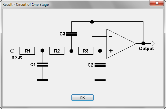
DACs need a reconstruction filter to remove unwanted frequencies. Here is an example that claims to be good:

https://www.analogfilters.com/high-quality-reconstruction-lowpass-filter-for-digital-audio/

Circuit

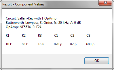
Components

https://www.softwaredidaktik.de/active-filters/download/

Saturday, December 28, 2019

Blofeld waveforms

I tried for a day or two to decode the PPG wave tape format, in hopes of seeing the original single cycle waveforms in there somewhere. I did get some traction on decoding the tape format itself, but never enough to find the waveforms.

Enter this:
http://synth.stromeko.net/Downloads.html

On this page it is possible to download the Blofeld User Wavetables. They are said to contain  among other things the ROM waves of the Prophet VS, MicroWave and SQ80. Only problem is, the site had them as a Blofeld sysex midi file only.

I couldn't find any sysex reader, but I found the next best thing, a project that converts wave files to Blofeld sysex files: https://github.com/alvare/wave2blofeld

Reversing the process, with some trial and error, and voilá - I now have a raw PCM file containing the waveforms in 16 bit signed little-endian single channel.

There are some issues though:
- In the original mid file there are some discontinuities, places where I would expect to find a sample at positive max, but instead find one at negative max. I suspect this is due to a rounding error when the mid file was created?
- Even after correcting for max-errors, there still seem to be places with error, but where the peaks are not completely at max.
- All samples are 21 bit in the midi file. I have truncated them to 16bit but as there is data in the  lower 5 bytes, we lose some precision.
- Some of the wavetables have very low amplitude, I suspect these could be doubled.
- Each sysex block has two more bytes right after the initial 0x70 than what is written by the wave2blofeld.

In general, the format is fairly easy. Each wave has its own sysex block. These start with:

[  0]: 0xF0[  1]: 0x83[  2]: 0x19[  3]: 0x3e[  4]: 0x13[  5]: 0x00[  6]: 0x12[  7]: wavetable num[  8]: wave num[  9]: 0x00

Wave data starts at byte 11. Each sample is three bytes long and the original 21bit sample can be


Wave data starts at byte 11. A wave is 128 samples long. Each sample is three bytes long and the original 21 bit sample can be recovered as

sample = (block[i] << 14) + (block[i + 1] << 7) + (block[i + 2])

To convert to a 16 bit value, simply shift right 5. ( >> 5). PS: Data is stored as 21 bit signed.

The wavetable name is found at block length - 18, and is 14 bytes long. Standard ASCII values are used.

The four last bytes are

[408]: 0x00[409]: 0x00[410]: checksum
[411]: 0xF7

Each wavetable consists of 64 waves and each wave is 128 bytes long.

PS: There is data between sysex blocks as well. If decoded, it reads something along the lines of 'Blofeld UserWT', and before each wave it says 'UWTxx wave yy' where xx is the wavetable position and yy is the wave number. I have not cared to look closer into this as it is unimportant for the waves.