Showing posts with label DAC. Show all posts

Monday, August 3, 2026

DAC on the same bus as DCO. Also, DCO nightmare...

As I'm preparing to put a 12bit DAC on the SPI bus shared with DCOs and the bit crusher, I had to make some changes to how to communicate with the DCO. 

 EDIT: I've written the code in a way that supports 3 bytes per DAC update so even 16bit DACs are supported in theory. For 12bit DACs, only two bytes are needed)

The DCO expected to receive three bytes with a 9us delay between sends and the CS line toggled only at the end of the last byte.

First I rewrote that, to accept single bytes. Then I changed the format so the first byte started with 1 and then had a fire bit command. The two last bits + 2 x 7 bits from the next made up the 16 bit frequency for example. That way, we can sync on the first byte instead, as it's the only one with a 1 as MSB.

Anyway, the bus can at best run at 4MHz when communicating with the DCO, or else each bit length becomes too short for the PIC16F. At 4MHz each bit is 0.25us long.

I want to run the DAC at 2ch * 48kHz = 96kHz. But if the DCO sends all its bytes in one go, it would take up too much time in a single period, preventing a stable DAC update frequency.

At the same time, I want to run the CV updater and DCO updates at 6kHz (well, ideally I wanted to update the CVs at 12kHz, but I can't seem to get a stable 192kHz interval (CV updating is split into 16 updates, 16 * 12kHz = 192kHz) so I think I have to settle for 96kHz. This fits well with the DCO which cannot be updated faster than 8kHz anyway, so 6kHz it is.

So, I came up with a system of 16 slots (96kHz/16 = 6kHz), each 1s/96000 or 10.4us long. The DAC can send its 3 bytes (with no delay between) in any slot, it would take slightly more than 6us. 

That leaves around 4us. Sending a single byte will take around 2us, so we can let any other peripheral send on the second half of the slot. Also, since DAC and DCO will be mutually exclusive (per channel), the DAC may send at the start and any other device (e.g. BC) in the second half. Also, by separating DCO frequency updates and DCO commands (sync, range etc) into separate slots, we can send both within a single 16slot cycle.

Anyway, I implemented this - and then the nightmare started.

The DCO had massive errors to the slope - every cycle overflowed, the saw was no longer a saw.

I spent almost two hole days debugging. Was it the protocol change, some previously untested code changes to the DCO or something in my controller code? 

Turns out, it's likely a problem with the MikroC compiler (again). When writing two chunks to the PIC internal FLASH rom, one with DAC values and one with DAC slopes, the values one got written to both positions! I am not sure if this started to happen now, but it would be weird if it has been that way for a long time.

The solution is to calculate the slope on the fly (it's simply a subtraction). But when I removed the code for writing the slope to FLASH, everything failed. So now I still calculate and write slopes during calibration, I just don't use it. 

I truly hate the MikroC compiler. I really need to port everything to MLabs.

In the process of figuring out what was going on, a few other things happened. First of all, one of the DCOs got stuck at a single frequency. Turns out, one of the SPI pins got pushed in/up through the board (cold solder joint probably). Then, another DCO simply didn't want to calibrate properly. It took a long time to realize that this only happens at the bottom end of the frequency spectre, around 40Hz and lower. At the moment, I think the DAC simply cannot supply a low enough voltage, so every cycle overshoots.

Then disaster struck. I put the DCO in the programmer backwards, sending +12V into one of the SPI  pins. The MCU still works, but SPI has stopped working so it's trash.

So right now I'm two DCOs short, and I have only one that can be calibrated down to the lowest frequency. Not sure what to do about that, but the others work down to around 40Hz which is good enough I guess. We'll see what the rest end up with.

Oh, and I managed to fix a long lasting bug - when changing to a lower frequency, the first cycle would end early because the previous interval's timer wasn't stopped. It seems to work fine now. 

BTW: I had another weird issue that I didn't get to the bottom of. One of the DCOs managed to reach all the way down to 4-5Hz, while the others only managed 8. I think 8 is right. Maybe the first one ran at half the expected speed (16Mhz instead of 32MHz)? 

BTW2: I first suspected that the overflowing waveform was caused by the interpolation between calibrated points being wrong. It did have something to it, the interpolation will be off by a few percent, bulging towards the end. But not as much as I saw. However, this lead me to try without any interpolation at all, just using the calibrated value for the start. That worked pretty well, it only sags by a few 10s of a volt at the end. Pretty interesting, by doubling the number of measured points we could maybe get away without the interpolation. 

BTW3: There is something strange at the startup of the DCO, when hammering the synth with midi, it feels like the DCO lags/hangs, before suddenly doing all the changes. This has not been investigated further.

Tuesday, July 21, 2026

Digital oscillators on the XM8

After deciding on creating a wavetable oscillator for the XM8, I've thought quite a bit about the digital oscillator structure. Here is my current solution


Two physical DACs

First of all, I will add a new PCM5102 I2S stereo DAC. This has built-in oversampling etc to prevent aliasing-noise. However, in old synths there were a lot of aliasing, which is part of what we now recognize as the vintage sound. I don't think the PCM5102 can recreate this.

However, my initial idea was to use the DAC8830 on the DCO boards for wave duties as well, and have the DCO MCU do the heavy lifting when it comes to wavetable morphing and other interpolation. The DCO DAC was then followed by an analog reconstruction filter.


The DCO as a DAC proxy

I now have a new idea. Let's instead use the DCO MCU as a simple DAC proxy. By copying the incoming SPI signal to the output whenever the DCO is in "direct to DAC" mode, the MCU doesn't have to do any work. We could probably speed up the SPI bus to max and easily get 44.1kHz (or 48kHz) sample rate on the DAC. The only thing left to solve is when to interpret the DCO incoming data as bytes directly for the DAC - we could increase bit length to 24 and use the first as command, but perhaps that makes it harder to use Teensy Audio. It should be possible to use custom SPI DACs with Teensy audio so let's hope this works. If not, there is still an available utility pin on the DCO that can be used for mode switching.

We would also have to send the chip select for the DAC, but only after two received bytes, not 1 as on the PIC16F SPI.

We can also get rid of the recon filter, after all the only reason we do it this way is to get the aliasing. Also, it would be possible to reduce the bit depth to 12bit if we want etc.


DAC routing

The analog board already has an input for digital waves per DAC, and a switch to select between that and the waveshaper output.

We can reuse that - and in place of the current reconstruction filter, we'll put a second switch selecting either PCM5102 or DAC8830. We also need the circuit to center and amplify the output from the DAC8830. Currently it's at 0 to 3v3. Finally, we need two available pins on the Teensy for controlling the switch.


Modifying the v1.0 Digital voice controller 

This requires the use of two additional pins on the recon filter socket - one for the PCM5102 input and one from the Teensy to control the switch. We should also cut the paths from the PCM5102 to the ext input (cut on the digital voice card side).


Summary

It will be possible to use one of three modes per oscillator: DCO, high quality audio DAC or aliasing basic DAC. It won't be possible to combine DCO with the other two at the same time on the same oscillator. I think this is a fair limitation that makes operation of the oscillators simpler - what you see is what you get, if you switch oscillator mode you also switch its output.


Sunday, June 28, 2026

Wavetable oscillator

I need a more precise sine wave than I have at the moment, with a larger range than I can get from the DCO.

That gave me an excuse to go ahead and create the wavetable/PCM oscillator I've been thinking about - there's a slot on the digital board exactly for this.

My colleague Alexander used a PCM5102A DAC for his project, and after taking a closer look it seems this was the ideal choice for my oscillator as well. Even better, I realised I had a breakout board with that DAC already, from Aliexpress, so I could go right ahead and test it!

Here is my layout:

CLK: GND

BCLK: Teensy pin 21

LRCLK: Teensy pin 20

DATA: Teensy pin 7


NB: All data/clock pins have a 22Ohm resistor on them to slightly slow down the edges. This is both suggested by the teensy communit (100Ohm) and the breakout board (22Ohm). 

The rest of the configuration pins are already taken care of on the breakout board, but in any case they are:


DEMP: GND (Deemphasis off)

XSMT: +Vpp (Soft mute: un-muted)

FMT: GND (I2S)

FLT: GND (normal latency) - I've made this configurable in my circuit


For the rest of the pins, see my schematic: 

I've added two inverting gain op amps that brings the output up to +/-5V. FLT (filter latency) is configurable and can also be disconnected from the control pin by cutting the solder jumper.


 I've already implemented wavetable morphing, through any number of wavetables. I've added the four basic waveforms (sine/tri/saw/square) and converted the Prophet VS wavetables into a format that I can use. It sounds amazing!

Right now the oscillators are routed through the ext pot. I originally intended wavetable oscillator duty to be performed by the DCO circuits, so there's a switch between DCO and waveform after the waveshaper on the analog board.

Now I'm not so sure anymore. It would be nice to not use the ext route. Instead, wavetable-osc could be routed directly to the mixer, and to have separate volume control per osc. Instead of having one channel per wavetable oscillator I could let one channel go to each of the busses. I can mix the oscillators digitally instead, and have digital volume control of them.

This is much more flexible. I can use both DCOs and WT at the same time, or I can make them mutually exclusive in software. The only issue is that DCO and WT have to share the same panel pot, meaning we no longer get knob-per-function if both DCO and WT are available at the same time. Then again, this could also be configurable... 

Monday, March 23, 2026

A little research into the startup problems

TL;DR: The DAC isn't starting up correctly, causing the CVs to either be the wrong value or to fluctuate.

There are two weird things that sometimes happen during startup. 

1) We get massive noise (but with a fixed frequency on the output

2) We get some kind of slew on the square wave, e.g. it is not flat on top.

Not sure if 2 happens at the same time as 1, but 2 can at least happen on its own


After a little measuring, I found that

1 comes from the waveshaper. It is present on all inputs but the DCO input is super clean.

2 comes from something between the square wave output of the waveshaper and the input of the bus mixer.

So what's between them? The waveform mixer and the oscillator output switch, but for the moment that's replaced with a jumper - so it's only the waveform mixer. It is implemented directly on the mainboard, except for the VCA chip.

Output on top, output from waveshaper on the bottom. WS looks good 


Input at the source mixer on the bottom. Here it's slanted.

The mixer PULA is the square wave input, the square wave amp sits before the pulse output on the waveshaper

This is interesting. The only thing between the waveshaper and the source mix board is that op amp. But the mixer also feeds into it, so maybe some of the other waveforms are leaking through?

Also note that the output wave has some strange spikes on it (the same ones for each cycle) that are not found on the mixer input. Approximately 12? 


Here is something more.

When square is slanted, triangle is not aligned:

The triangle does not match up

 
Triangle with a good signal

Trims when slew: 2.0, 2.8V (center, symmetry)

Trims when clean: 2.3, 3.0V (these are also what is expected).


Let's look at the DAC


With slew

DAC ref voltage: 2.1 to 2.386

Output on DAC ref voltage pin, too low and fluctuates


Output on one of the channels, is too low


When clean

DAC ref voltage 2.5V 

DAC ref voltage is perfect

Output on the same channel as above. Looks good.


DAC +5V and GND inputs are clean even with slew


As for resetting the issue - turning off and waiting a short time had no effect. But quickly turning off and on made it go away.

The errors appear without turning off +5V, only +/-12V. 

On some rare occations the output flatlines on startup. On a single one, DAC output latched at something else than 0 (?) and a mix of two sources (?) could be seen on the output.

With the new seventyPWR, I have only been able to reproduce case 1 two times. It may be caused by the DAC too?

Edit: I managed t reproduce the extremely noisy case after reconnecting the old PSU and running two voice cards.

GND on the DAC is stable, the +5V very slightly wobbles, but nothing extreme.


The Vref however, is 4.23V, way too high:


DAC ref voltage should be 2.5V but is 4.23! Also note that the noise on the voice output is following the same pattern for each cycle, it's not random noise

The DAC output looks like it follows the correct "pattern" but the amplitude is of course way too high too.


DAC output is higher than it should

Now, as for the waveshaper - DCO input looks as it should, but everything else is garbage. Interestingly, the symmetry and center trim inputs are not stable voltages, but jump up and down. Moving further down the signal path, the mixer input channel 2 CV is also not stable. 

Mixer input channel 2 CV

Waveshaper 2 center CV

Waveshaper 2 symmetry CV

Waveshaper 1 center CV

Waveshaper 1 symmetry CV


It simply looks like the CV mux is not able to generate stable CVs, either because the clocking is wrong or because the DAC output is too high, making it settle at the wrong voltage. In other words, the massive noise is ALSO caused by the DAC. That's nice to know!

Tuesday, May 20, 2025

Thoughts on VCO CV resolution

In the current version of the XM8 voice controller, the 5V CV is meant to span 13 octaves for the VCO. I am however starting to worry that the span is too large / the CV not precise enough for this to work, so here are some possible solutions to improve that, followed by some calculations about precision that may or may not make sense!

Now, most VCOs have a  1V/oct response, and we have a 5V CV range. This means that the normal configuration gives us 5 octaves (without any tuning, that is)

Update: The Prophet 5, from which I've stolen my VCO design, uses 10V CV. More on this at the end.

What can we do about the range?

We can introduce a second CV to select octave range. Lots of synths transpose the VCO up/down this way. If we use a second 1V/Oct input, we can get 5 more octaves (just not at the same time).

We can even build a circuit that is easily modified between 13 and 5 octaves like this:

a 100k and 56k in parallel gives around 36k ohm, which in turn gives us around 13 oct of range. Cutting JP5 makes the input 100k or 5 octaves.


Now, this will improve the resolution of the CV. It will also make the CV less susceptible to noice (by a factor of 2.5). But from my measurements, some of the noise is even present in the CV itself. And adding two CVs with the same noise will double it, and the improvement is only a factor of 1.25. 

Can the noise issue be improved?

Here is a possible solution: Invert the second CV (and shift it upwards by 5V). Everything is computer controlled, so re-inverting in software is no problem. Summing these CVs will cancel any common noise. Of course, if the noise is present in the summer or shifting voltage as well this won't help, but I suspect that the noise I've seen originates from the SPI signal controlling the CV DAC. 


Now for some calculations

With a 16bit dac, the theoretical number of discrete steps is 65536. When controlling 13 octaves, a semitone is 65536 / (12*13) = 420, meaning a minimum interval of 0.24 cents. But one step is also 5V / 65536 = 0.076mV, which is extremely small! Any noise will greatly affect the CV. For example, a noise peak of 1mV equals 13 steps or 3 cents. This is around the limit of what the human ear can discern.

One is often saying that a more realistic resolution is 14bit, in which case one step is 0.3mV. Now the max resolution is 16385 / (12 * 13)=105, or about one cent. Still ok, but close to what the human ear may hear.

So what happens if we reduce the VCO range to 5 octaves?

A normal VCO has a 1V/oct input. In this case, 5V spans 60 semitones or 6000 cents. In other words, one cent is 0.83mV. A 1mV error means a 1.2 cent pitch error, or 2.5 times better (which should hardly be a surprise as 13/5 = 2.6). As for tuning, a 14 bit dac will get 16384/60=273 steps per semitone or 2.73 steps per cent. Again, 2.5 times improvement over the 13 octave case.

All in all, using a 5V span lets us use a 13bit effective resolution and still get around 1 cent resolution. It is also less sensitive to noise - at the cost of only being able to span 5 octaves instead of 13. It also means that I have no way of offsetting or correcting for linearity errors, which may make this a bad idea. I could use the second CV for offset, but then I would also reduce the number of octaves available.


Update: The Prophet 5

So, after posting, I had a closer look at the original circuit diagram for the Prophet 5. On electric druid, there's a comment about the P5 not using the HF tracking input, but instead probably doing corrections through the digitally controlled CV.

But that had me thinking - if the CV is 0-5V, there's no room for tuning. Turns out, the P5 CV is not 5V, it is 0-10V directly from the DAC, leaving plenty of room for tuning etc! It uses a 16bit DAC, though the two lowest bits are left out as it is only 14bit monotonic.

A 10V output from the DAC means that we have twice the range of a 5V CV, but without a higher noise level. E.g, 100mV noise on the 5V CV with a 5 oct range is the same as 100mV noise on 10CV with 1= oct range. The steps-per-cent is the same. 

My case is actually even worse. I have a 2.5V DAC which is then amplified to 5V. Any noise present at the DAC amplifier will be doubled. So, instead of having a 10V CV span 10 octaves, I'm trying to make 2.5V span 13. 

So, depending on where noise is actually introduced, I have a possible CV noise level  5.2 times higher than the Prophet 5. Damn.


Thursday, November 14, 2024

Testing the CV generator card

I've finally started testing the new cards. First off is the 56 channel CV generation card.

After first testing the 4ch DAC on a breadboard, driving the old 16ch sample and hold cards, and making sure the code ran perfectly on that, I connected the DAC to the CV board and the CV board to a Teensy 4.0 and...

...nothing.

No output at all on the output pins.

A quick check in Eagle revealed the first major bug - I've forgotten to connect the rear row of the connectors, only the front one is connected. Not a problem for testing but it will require a lot of soldering to bridge all the 56 outputs. 

I then switched to the rear pins and...

...again, nothing.

Damn. I do however try to run the DAC at 50MHz and 5V logic supply, from a 3v3 Teensy. It wouldn't be surprising if that lead to some issues.

 I left the card for a few days and returned yesterday. This time I disconnected the DAC and put it on a separate breadboard, running 16 wires over there. I could then connect probes to the inputs and outputs to see if the DAC itself was actually doing anything.

And what do you know, this time everything worked immediately! Very strange. Perhaps the long wires or the connected probes changed something.

Thus, today, I moved the DAC back to the CV board, but left it slightly high to be able to connect clip on probes onto the DAC board pins while it was inserted into the CV board. And this time it worked!

Finally, I disconnected the probes, one by one. When I got to the probe on the SPI clock pin, everything stopped working. I reconnected it and disconnected all the rest, and it started working again.

As a last try, I connected the probe to the other end of the SPI clock wire, close to the teensy. This time it stopped working too.

Sooo... not sure EXACTLY what is going on, but perhaps the added load/capacitance of the probe slows down or filters the clock slightly?

Anyway, once I got everything working, the output looks great!

Closeup of one of the outputs shows a fairly stable level, the noise seen is 0.005V which is most likely the minimum step on the scope ADCs.


Four simultaneous outputs


Update:

I've tested all channels and they work great. I also tried reducing the SPI speed to 25MHz to see if that changed anything with regards to needing the probes on the clock bus but it didn't help.

I did notice too that the sample and hold op amps get very hot but I experienced the same on the previous 16ch board so I'm not too worried.


Logic level converter

I have designed a small 4 channel logic level converter board based on the TI SN74LVC2T45 IC. It will translate the 3v3 Teensy level to the 5V the DAC expects. I use 5V on the DAC as that's necessary to run at 50MHz.

Most level converters are way too slow for 50MHz, but the TI chip datasheets says that 420 Mbps is possible when doing 3.3V to 5V translation. We'll see.

I also have the option of rewiring the CV board by cutting a jumper and soldering another one, to make the DAC run at 3V3. My most recent breadboard tests seemed to show that it would be possible but it DOES feel a bit risky for a final design.

Tuesday, June 18, 2024

DAC8565 and 16ch sample and hold

I intend to use the DAC8565 quad 16 bit DAC for the XM8, I've even bought 20 of them on breakout board and written a test - but for some reason, I haven't written anything about it.

Right now I'm making the final CV mux board, so I had to retest my program. For some reason though, it doesn't complie anymore?

In my code I'm using SPI.send24 as well as SPI.hasInterruptFlagSet, SPI.clearInterruptFlag and SPI.enableInterrupt. 

I can't find ANYTHING about send24 anywhere, and very little about the others. But I found another SPI project locally, SPI-master, that has the send24 code. It says it is from https://www.pjrc.com/teensy/td_libs_SPI.html, but going there leads nowhere. Not sure what has happened, I feel completely gaslit!

Anyway - I copied the SPI-master into my project to get send24. As for the interrupt stuff, it's not really necessary as it only makes it possible to listen to send completes to trigger Load dac - and this can be done in software without penalty anyway, by adding it to the setting of the last DAC channel.


Ok, so how do we use the DAC8565.

The following pin config works:

pin 1,2, 7 and 8 are the four output channels

pin 3, Vref H, is the high reference voltage. It outputs the internal reference voltage (2.5V) if the internal voltage reference is used, and should be connected to ground through a 150nF cap. If using an external voltage reference instead, it can have an additional 4.8uF (!) cap to ground for reduced noise.

It is important to note that the max output when using the internal reference is 2.5V. To get a 5V output, we need to use an external 5V reference.

It is also important to note that the external reference CANNOT be higher than the Analog voltage AVDD, or the output will be clipped. 

Pin 4, AVdd, power for the analog parts. It may be 3v3 if using the internal 2.5V reference as output, or 5V if using an external reference.

Pin 5, Vref L, the low reference voltage. Usually connected to GND

Pin 6, GND

Pin 9: !Sync. = SPI Chip select

Pin 10: Serial clock

Pin 11: D in, Serial data. Connect to master MOSI

Pin 12, IOVdd. This should match the logic level of the MCU, which for the Teensy is 3v3. However, I had some success setting this to 5V even with 3v3 output, but I get glitches when running the SPI bus at 50MHz. Also, it says in the spec sheet that 3v3 logic has a max bus speed of 25MHz (I have successfully used 50MHz on the current breadboarded circuit, and 46MHz earlier, but IOVdd must be 3v3.

I will try using 5V logic but that requires a high speed level shifter between the Teensy and the DAC.

Pin 13: !RST - when set to 0, all DAC outputs are reset to the value of RSTSEL

Pin 14: RSTSEL - reset select. If 0, DACs power up and reset to 0, if 1 they reset to the middle of the reference voltage.

Pin 15: !Enable - "Connects the SPI interface to serial port". This is currently confusing me though connecting it to 0 works fine.

Pin 16: LDAC: Load Dac. Connect to GND and control this through software or connect to MCU


Running a loop with IOVdd at 3v3, AVdd at 5V and using a 5V external reference

50MHz SPI works fine


There is significant noise on the output

The noise is however only while the SPI bus transfers. This may make it bearable even if present in the real circuit, as we can transfer the data and let the signal settle before turning on the output muxes that load the sample and hold caps.

5V IOVdd also works...

Unfortunately, we get glitches at 5V IOVdd

The glitches go away when reverting to 3v3IOVdd


With MUX

I spent a long time trying to get my 16ch CV buffer to work with the DAC. Turns out I had mislabeled pin D0, it should be next to D1, not next to GND. 

Anyway, once I got that out of the way, the 16ch board works fine:

DAC Output through opamp buffer and 470R to mux. Works great!

Output is very stable. DAC slightly overshoots when switching (meastured after the buffer I think)


I tried various combinations:

5V external reference, 470Ohm resistor directly to DAC

5V external reference, no resistor, DAC directly to mux. DAC has no problem driving the charging

2.5V internal reference, 2x positive gain op amp, 470R input resistor

5V external reference, 470R input, no buffer. Something is very wrong! Not sure exactly what.

Some closeups

Extreme closeup of 2.5V ref through 2x gain and 470R resistor.

Extreme closeup of 5V ref, buffered and 470R resistor. Pretty much the same

Extreme closeup of 5V ref direct from dac without resistor. A tad noisier?

Then some charge times:

Dac output when run as 5V ref direct from DAC without resistor. Rise time is around 5.5uS

5V ref direct from DAC without resistor. Charge time 0 to 5V for CV buffer cap. Around 1.5uS

This is as far as I got, because here I somehow killed the Teensy :-( I would have liked to have the same two checks when running with 2.5V internal reference and 2x gain through 470R. Have to look for a new Teensy

...oh, I found one. Let's go on

Cap charge time through 470R resistor, around 3.4uS

But what if we change to a 220R instead?

Cap charge time through 220R resistor, around 2.2uS


That's pretty good. Let's look at the DAC settling time:

Rise time from 0 to 5V, as seen at the output of the buffer after the DAC, is around 2.9uS. The drops in voltage coincides with the charging of the caps and are not present at the DAC output.

All in all, this looks very promising. For my first production version I will use a 2x positive gain buffer with a 220R charging cap.

Wednesday, February 1, 2023

DAC and ground in multicard systems

Now this has been a big mystery to me for a long time.

DACs tend to have two ground pins - digital and analog ground. It's not an insane thought to think that these should be connected to different ground planes. 

Reading up on this previously, the mantra has been that you could do this, but then the two ground planes should be connected under the DAC.

While this may be fine for a single DAC system, where the DAC is the only point where analog and digital meet up, my system is definitely nothing like this. I have multiple DACs on a single card, and multiple cards in the system. 

Connecting two DACs this way, with the grounds connected under both DACs, would (at least in my mind) create a ground loop which is not desireable. So what should a poor designer do?

Today I found this document: 

https://www.analog.com/media/en/training-seminars/tutorials/MT-031.pdf

"Grounding Data Converters and Solving the Mystery of "AGND" and "DGND" (MT-031)

It describes in detail how to approach this, including the multi-card issue. A short short summary is:

- AGND and DGND _pins_ should both be connected to AGND at the package
- If V_digital is not the same voltage as V_analog, V_digital should be decoupled to AGND
- AGND and DGND planes should be connected at each card through Schottky diodes to prevent a potential difference buildup

There are a lot of other considerations and preconditions that have to be met, but this at least provides some good guidelines and explanations.

Ferrite beads

One advice still troubles me a bit though. Using ferrite beads. They seem like the magical solution. The problem however, is that every DIY'er out there treat them like they are all created equal. I did read about this earlier and it seems this is not at all true - you have to know a lot more about your circuit and pick the correct bead. Without this, you just waste money and board space. 

I'll see if I can find more about this later.

Thursday, July 21, 2022

DAC8565

I had some DAC8565 (quad 16bit DAC) breakout boards made at JLCPCB, and just tested them, they work fine.

The datasheet says that SPI speed for < 3.6V Vdd is limited to 25MHz, above that it's 50MHz. I am able to run the SPI at 45MHz at 3v3 though, and it seems stable. 50MHz does NOT work.

Here are my connections for using the internal 2.5V reference. It is especially important to note that the VrefL must be connected to ground even if using the internal reference:

1: VoutA
2: VoutB
3: VrefOut: 150nF to GND
4: AVdd: 3v3 + 100nF decoupling cap to GND
5: VrefL: GND
6: GND
7: VoutC
8: VoutD
9: !SYNC: SPI CS
10: SCLK: SCLK
11: Din: MOSI
12 IOVdd: 3v3
13: !RST: 3v3
14: RSTSEL: GND (binary input)
15: !ENABLE: GND
16: LDAC: GND or pin on MCU if doing hardware LDAC, this can also be done using a command.


Thursday, March 31, 2022

Saving the DCOs

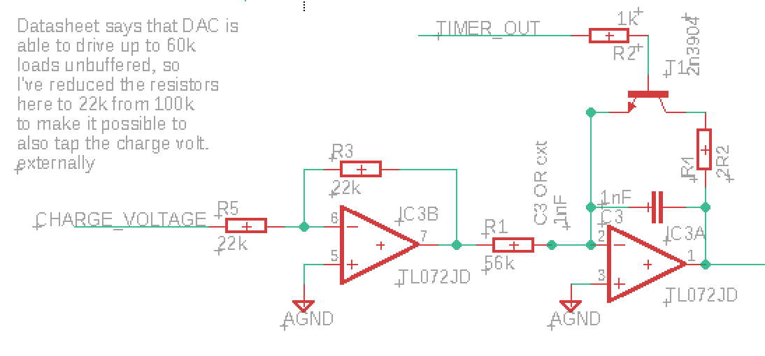
I've posted about this before, but I did a crucial mistake in rev 1.4 of the DCOs. Unfortunately, I also ordered a full set of them (40x) and the microcontroller and DAC (DAC8830) I used have since become unavailable at JLCPCB, so I can't just order a replacement.

My mistake was that I reduced the resistor the DAC outputs through from 100k to 22k, thinking that it had to be less than 60k when in reality it should be MORE THAN 60k.

I need to replace R5 with a 60k resistor

Fixing this means desoldering at least one resistor, but after that I have some options.

The "correct fix"

The correct fix would be desoldering R3 and R5 and replace them with new 60k resistors. It is a bit finicky to do this, especially removing R3 will be hard. (UPDATE: Even this would not make the output perfect, see Update 3 below)

Easier fixes (?)

The DAC feeds into an inverting op amp with unity gain (Rf = Rin = 22k). 

By replacing only Rin with a 60k resistor, I would get an inverting amplifier that attenuates the signal to -Rf/Rin = -22k/60k = -0.37.

Unfortunately, attenuating inverting amps are known to self oscillate. The solution, as described here and here, is to put a resistor of the same value as Rf from the negative input to ground. 

There are a few ways to add this resistor. 

First, I may add it directly between leg 5 and 6 on IC3. It may be possible to use a 0603 resistor, or at least a 0402 directly, but it may be a bit hard.

IC3 pins 5 and 6 are in the lower right corner


Second, I may desolder R5 and put a tiny wire from the top pad to pin U1 (utility 1). Doing things that way means I could add a replacement for R5, as well as a resistor to ground, on the board the DCO plugs into. 

Charge current

Since the output from the inverting op amp now is much smaller, I also need to place a resistor in parallel with R1 to increase the capacitor charging current. I need to do this anyway, as the DAC output in my original design was 5V, but running the DCO from 3.3V means the DAC output now can never reach above 3.3V. 

Another option would be to simply amplify the DCO output. I do this right now on my prototype, I need to do some calculations and experimentation here to see what is the best solution.

Change nothing

The last option I have is to do a bit of measuring on the DAC output. When do we run into problems? Is the max 60kOhm load rule for the whole range or just for the higher values? Is it related to the output current?

If it is indeed current related, we may have a few options. First of all, maybe reducing the reference voltage, which in turn reduces the output current at max, is enough? 

Similarly, if the higher values are the issue, could I get away with using only 15 bits, leaving the MSB at 0? Testing is needed!

Update 1:

Measurements from the DCO


This is weird. I did a lot of measurements and calculations. The DAC voltages follows the pitch, no errors as we go up the scale (apart from some tiny errors at the bottom that may as well be with my probes).

However, I have connected 3.3V as Vref. According to my calculations this means the output voltages are off by 25%. BUT - when I replace Vref with 2.5V in my spreadsheet, I get exactly the output I see on the dac! The error is around 0.5%, and that's to be expected since I haven't included the slope part of the lookup. This is SO weird. I need to look at this again tomorrow.

Update 2:


Changing to a 2.5v reference made the max value drop from 2.17 to 1.66V (Expected is 2.84 and 2..16 respectively). The diff is still 23% and it is still consistent across the DAC range.

Next up: breadboard a new circuit and check if the output changes (and at what rate) when changing the resistor.

PS: the DAC output impedance is approximately 6.25 kΩ

Update 3:

I did some measuring during my lunch break, and the results are extremely uplifting:

I replaced the input resistor Rin and measured the DAC output for various values. Then my hunch told me to compare it to what would happen if we measured the mid point of a resistor divider between Vref and GND, where the top resistor is equal to the DAC output impedance (6.25k) and the bottom resistor is equal to Rin. 

The two voltage columns speak for themselves - it is clear that this is what is going on. This means that
- The output will probably be exactly the same between the various DACs I'm using
- Even if I changed to a 60k resistor, I would not get a perfect result

In other words, I can probably just leave the 22k Rin as it is, and compensate in the charging resistor part instead! This is just amazing!

Even better, I added a buffer after the DAC, to see if tapping the output for my wave player idea affects the output, and it absolutely doesn't :)

Update 4:

I tested connecting a resistor in parallel with R1 to increase the charging current. Originally I intended the max charging current to be 5V / 56kΩ = 89.3uA. Now the max DAC output is 1.94V if we use a 2.5V reference, so we need R1 to conform to 1.94V / R1 = 89.3uA, meaning R1 has to be 21725Ω. By putting a resistor in parallel with the current R1 we can lower the combined resistance - to get a combined resistance of 21.7kΩ the second resistor needs to be 35.5kΩ. If we choose a 36kΩ resistor, the combined resistance is 21.9kΩ and the current 88.6uA, fairly close to the ideal.

I tested this, and the wave amplitude instantly jumped to 9.4V (With a 3.3V reference, it passes 10V. The tops are cut off but I assume that is because the calibration output (connected to the microcontroller) is > 3.3V, I've seen this happen before).

So - all I have to do to make the DCOs work properly - with a 2.5V reference instead of 3.3V btw - is connecting a 36kΩ resistor in parallel with R1, and 75kΩ and 3.3kΩ resistors (in series, so 78.3k) in parallel with R7 to get the correct value at the MCU calibration pin - see https://atosynth.blogspot.com/2022/01/big-bug-weekend.html for calculations of R7


Increasing max frequency


Right now, the DCO has a range of 8Hz to 8kHz. I want to move this to 16Hz-16kHz (or 20Hz-20kHz).

This can be done either by decreasing C3 from 1nF to 500pF (560pF may be the closest option), or by changing the value of the resistor in parallel with R1:

We now need the max charging current to be 178.6uA, meaning R1 should be 10.86kΩ. The necessary parallel resistor would be 13.4kΩ. It is better to choose a slightly lower value than a too high one, so 12k may be the best standard value.

Update 5:

By swapping R1 with a combined resistance of 14.5kΩ and using a Vref of 2.5V I'm able to cover the full midi range (8Hz to 13.3kHz) with only 3 cent errors on the highest pitches. This does not leave room for pitch bend at top/bottom, but each note is exactly 512 steps up from the previous which is a nice number to work with in the voice controller.

Reducing to 9.1kΩ lets us add another 12 semitones, giving us a range of 5Hz to 21kHz, though I'm not sure it's worth it.

All in all, I think I should consider making a bootloader for the DCOs, there are so many things that could be changed after install, and having to manually change 16 (or 32!) of them would be a real pain.