Showing posts with label DAC8830. Show all posts

Tuesday, July 21, 2026

Digital oscillators on the XM8

After deciding on creating a wavetable oscillator for the XM8, I've thought quite a bit about the digital oscillator structure. Here is my current solution


Two physical DACs

First of all, I will add a new PCM5102 I2S stereo DAC. This has built-in oversampling etc to prevent aliasing-noise. However, in old synths there were a lot of aliasing, which is part of what we now recognize as the vintage sound. I don't think the PCM5102 can recreate this.

However, my initial idea was to use the DAC8830 on the DCO boards for wave duties as well, and have the DCO MCU do the heavy lifting when it comes to wavetable morphing and other interpolation. The DCO DAC was then followed by an analog reconstruction filter.


The DCO as a DAC proxy

I now have a new idea. Let's instead use the DCO MCU as a simple DAC proxy. By copying the incoming SPI signal to the output whenever the DCO is in "direct to DAC" mode, the MCU doesn't have to do any work. We could probably speed up the SPI bus to max and easily get 44.1kHz (or 48kHz) sample rate on the DAC. The only thing left to solve is when to interpret the DCO incoming data as bytes directly for the DAC - we could increase bit length to 24 and use the first as command, but perhaps that makes it harder to use Teensy Audio. It should be possible to use custom SPI DACs with Teensy audio so let's hope this works. If not, there is still an available utility pin on the DCO that can be used for mode switching.

We would also have to send the chip select for the DAC, but only after two received bytes, not 1 as on the PIC16F SPI.

We can also get rid of the recon filter, after all the only reason we do it this way is to get the aliasing. Also, it would be possible to reduce the bit depth to 12bit if we want etc.


DAC routing

The analog board already has an input for digital waves per DAC, and a switch to select between that and the waveshaper output.

We can reuse that - and in place of the current reconstruction filter, we'll put a second switch selecting either PCM5102 or DAC8830. We also need the circuit to center and amplify the output from the DAC8830. Currently it's at 0 to 3v3. Finally, we need two available pins on the Teensy for controlling the switch.


Modifying the v1.0 Digital voice controller 

This requires the use of two additional pins on the recon filter socket - one for the PCM5102 input and one from the Teensy to control the switch. We should also cut the paths from the PCM5102 to the ext input (cut on the digital voice card side).


Summary

It will be possible to use one of three modes per oscillator: DCO, high quality audio DAC or aliasing basic DAC. It won't be possible to combine DCO with the other two at the same time on the same oscillator. I think this is a fair limitation that makes operation of the oscillators simpler - what you see is what you get, if you switch oscillator mode you also switch its output.


Thursday, March 31, 2022

Saving the DCOs

I've posted about this before, but I did a crucial mistake in rev 1.4 of the DCOs. Unfortunately, I also ordered a full set of them (40x) and the microcontroller and DAC (DAC8830) I used have since become unavailable at JLCPCB, so I can't just order a replacement.

My mistake was that I reduced the resistor the DAC outputs through from 100k to 22k, thinking that it had to be less than 60k when in reality it should be MORE THAN 60k.
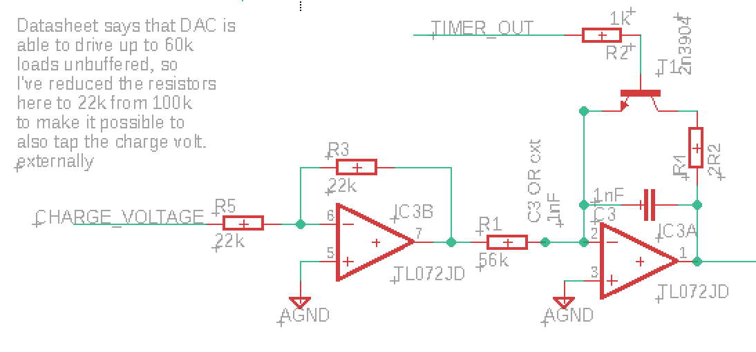
I need to replace R5 with a 60k resistor

Fixing this means desoldering at least one resistor, but after that I have some options.

The "correct fix"

The correct fix would be desoldering R3 and R5 and replace them with new 60k resistors. It is a bit finicky to do this, especially removing R3 will be hard. (UPDATE: Even this would not make the output perfect, see Update 3 below)

Easier fixes (?)

The DAC feeds into an inverting op amp with unity gain (Rf = Rin = 22k). 

By replacing only Rin with a 60k resistor, I would get an inverting amplifier that attenuates the signal to -Rf/Rin = -22k/60k = -0.37.

Unfortunately, attenuating inverting amps are known to self oscillate. The solution, as described here and here, is to put a resistor of the same value as Rf from the negative input to ground. 

There are a few ways to add this resistor. 

First, I may add it directly between leg 5 and 6 on IC3. It may be possible to use a 0603 resistor, or at least a 0402 directly, but it may be a bit hard.

IC3 pins 5 and 6 are in the lower right corner


Second, I may desolder R5 and put a tiny wire from the top pad to pin U1 (utility 1). Doing things that way means I could add a replacement for R5, as well as a resistor to ground, on the board the DCO plugs into. 

Charge current

Since the output from the inverting op amp now is much smaller, I also need to place a resistor in parallel with R1 to increase the capacitor charging current. I need to do this anyway, as the DAC output in my original design was 5V, but running the DCO from 3.3V means the DAC output now can never reach above 3.3V. 

Another option would be to simply amplify the DCO output. I do this right now on my prototype, I need to do some calculations and experimentation here to see what is the best solution.

Change nothing

The last option I have is to do a bit of measuring on the DAC output. When do we run into problems? Is the max 60kOhm load rule for the whole range or just for the higher values? Is it related to the output current?

If it is indeed current related, we may have a few options. First of all, maybe reducing the reference voltage, which in turn reduces the output current at max, is enough? 

Similarly, if the higher values are the issue, could I get away with using only 15 bits, leaving the MSB at 0? Testing is needed!

Update 1:

Measurements from the DCO


This is weird. I did a lot of measurements and calculations. The DAC voltages follows the pitch, no errors as we go up the scale (apart from some tiny errors at the bottom that may as well be with my probes).

However, I have connected 3.3V as Vref. According to my calculations this means the output voltages are off by 25%. BUT - when I replace Vref with 2.5V in my spreadsheet, I get exactly the output I see on the dac! The error is around 0.5%, and that's to be expected since I haven't included the slope part of the lookup. This is SO weird. I need to look at this again tomorrow.

Update 2:


Changing to a 2.5v reference made the max value drop from 2.17 to 1.66V (Expected is 2.84 and 2..16 respectively). The diff is still 23% and it is still consistent across the DAC range.

Next up: breadboard a new circuit and check if the output changes (and at what rate) when changing the resistor.

PS: the DAC output impedance is approximately 6.25 kΩ

Update 3:

I did some measuring during my lunch break, and the results are extremely uplifting:

I replaced the input resistor Rin and measured the DAC output for various values. Then my hunch told me to compare it to what would happen if we measured the mid point of a resistor divider between Vref and GND, where the top resistor is equal to the DAC output impedance (6.25k) and the bottom resistor is equal to Rin. 

The two voltage columns speak for themselves - it is clear that this is what is going on. This means that
- The output will probably be exactly the same between the various DACs I'm using
- Even if I changed to a 60k resistor, I would not get a perfect result

In other words, I can probably just leave the 22k Rin as it is, and compensate in the charging resistor part instead! This is just amazing!

Even better, I added a buffer after the DAC, to see if tapping the output for my wave player idea affects the output, and it absolutely doesn't :)

Update 4:

I tested connecting a resistor in parallel with R1 to increase the charging current. Originally I intended the max charging current to be 5V / 56kΩ = 89.3uA. Now the max DAC output is 1.94V if we use a 2.5V reference, so we need R1 to conform to 1.94V / R1 = 89.3uA, meaning R1 has to be 21725Ω. By putting a resistor in parallel with the current R1 we can lower the combined resistance - to get a combined resistance of 21.7kΩ the second resistor needs to be 35.5kΩ. If we choose a 36kΩ resistor, the combined resistance is 21.9kΩ and the current 88.6uA, fairly close to the ideal.

I tested this, and the wave amplitude instantly jumped to 9.4V (With a 3.3V reference, it passes 10V. The tops are cut off but I assume that is because the calibration output (connected to the microcontroller) is > 3.3V, I've seen this happen before).

So - all I have to do to make the DCOs work properly - with a 2.5V reference instead of 3.3V btw - is connecting a 36kΩ resistor in parallel with R1, and 75kΩ and 3.3kΩ resistors (in series, so 78.3k) in parallel with R7 to get the correct value at the MCU calibration pin - see https://atosynth.blogspot.com/2022/01/big-bug-weekend.html for calculations of R7


Increasing max frequency


Right now, the DCO has a range of 8Hz to 8kHz. I want to move this to 16Hz-16kHz (or 20Hz-20kHz).

This can be done either by decreasing C3 from 1nF to 500pF (560pF may be the closest option), or by changing the value of the resistor in parallel with R1:

We now need the max charging current to be 178.6uA, meaning R1 should be 10.86kΩ. The necessary parallel resistor would be 13.4kΩ. It is better to choose a slightly lower value than a too high one, so 12k may be the best standard value.

Update 5:

By swapping R1 with a combined resistance of 14.5kΩ and using a Vref of 2.5V I'm able to cover the full midi range (8Hz to 13.3kHz) with only 3 cent errors on the highest pitches. This does not leave room for pitch bend at top/bottom, but each note is exactly 512 steps up from the previous which is a nice number to work with in the voice controller.

Reducing to 9.1kΩ lets us add another 12 semitones, giving us a range of 5Hz to 21kHz, though I'm not sure it's worth it.

All in all, I think I should consider making a bootloader for the DCOs, there are so many things that could be changed after install, and having to manually change 16 (or 32!) of them would be a real pain.

Saturday, March 13, 2021

OB-6 CV generation revisited

After getting the closeups of the OB-6 it's time to put together what I've learned so far.

Hardware

1) The DAC used is AD5668, an 8 channel 16bit DAC with built in voltage reference (2.5 x 2 = 5V). The chip used by Sequential is the AD5668-3 that resets to midscale (2.5V). 

2) The multiplexers are TI CD74HCT4051

3) The op amp buffers are most likely TL06x as that's about the only thing found on the voice card

4) There is no DAC output buffering op amp as that is built into the DAC.

5) I'm not sure what size of sample and hold caps they are using


Timing/performance

Brian from Abstrakt Instruments has a great breakdown of how the refresh is done here:

https://youtu.be/4WwXlRYw_S0?t=1937

Each DAC channel updates 8 cv channels at 24kHz meaning

  • DAC channels are updated at 192kHz
  • There is about 5.2uS available for refreshing a single CV, this includes time to set the DAC, cap charging and any propagation delays/slew through the mux.
  • From the oscilloscope output, a full rail to rail change takes around 3uS

DAC performance

  • The DAC has a max SPI speed of 50MHz, meaning one bit takes 20nS to transfer. Each update is 32bits long, meaning updating 8 channels takes at least 32 * 8 * 20nS = 5120nS = 5.12uS.
  • Settling time is typically 2.5uS, but can be as bad as 7uS. (But it is stated that this is 1/4 to 3/4 settling so that means that it is only a change of 2.5V?)
  • Slew rate is 1.2V/uS

Multiplexer performance

  • On resistance is 90-180Ohm (?)
  • Propagation delay from in to out is 4nS, higher with higher capacitive load but still in the nS range
  • Switch delay is around 20nS
  • Charge injection: does not say.

What does this mean in practice: 


Well, we've got 5.2uS to update a single CV. First of all, if updating all channel takes 5.1uS, this cannot be done during that period. We want to update all channels at once, if we didn't we would need separate address lines for all the multiplexers which is infeasible. 

Luckily the DAC has a LDAC pin. This means we can write data to all channels, and when ready, flip the LDAC and load channels at the same time. By writing the next update while the current one charges the capacitors, we have just enough time to do a full 8ch update. We will also have to use hardware "fire and forget" SPI, writing the necessary 32 bytes of data in the background. If we use blocking SPI, we will have no time left between updates to calculate the next bytes!

Next, we still have to let the dac settle before we turn on the multiplexer output, or we would see an error in the voltage. Settle time is, from both the oscilloscope photo and the datasheet, around 3uS, but it could be as bad as 7uS. I would also think that the slew rate of 1.2V/uS also means that it would take around 6uS for a 5V change.

The multiplexer propagation delay is negligible. That leaves 2uS for charging the cap and turning off the mux again. 

Now, as I've noted in earlier posts, I could charge a 10nF cap rail to rail at 40kHz from a TL072, meaning charge times are around 25uS.  2uS means we need to use a cap at least 1/10th that size, or less than 1nF. 

I did some tests with the DAC8830 and a DG408 multiplexer. Using a 1nF cap did NOT let us fully charge the cap rail to rail in the 5.2uS window.  I got close but not close enough. The AD5668 may be able to deliver more current but that remains to be tested. 

So what do I make of all this? 


I suspect that Sequential is "cheating" here. They haven't spec'ed their system for charging rail to rail in <5uS, as they don't have to! The fastest moving signals would be the envelope attacks, and those NEED intermediate steps to sound good (?). 

I have ordered both the AD5668, CD74HCT4051 and TL072. It will be exciting to see the results of using those parts. Will I still have the charge injection issues? Does the AD5668 charge the caps faster? I will definitely post the results!