Showing posts with label VCA. Show all posts

Monday, July 7, 2025

Debugging VCO Pitch unstability continued 4 - selected solution

I've officially come to the conclusion that I'm not able to make the noise level any better at the moment. I've ended up at a point where the noise is at around +/-3-5 cents as measured at the VCO frequency. I'll list some of the things I've tried and what my selected solution is.

What causes the noise

The main parts of the noise seems to be caused by the current running through the transistor collector and to ground. The noise follows the pulse width. When the pulse VCA CV is turned down, the noise is reduced, from +/-14 to 3 cents. 

1k collector resistor, massive noise on VCO, and it follows the pulse wave (top)

 
With pulse VCA at 0, the noise is reduced

By increasing the collector resistor from 1k to 47k, the noise is greatly reduced. The noise is still present even if the pulse wave VCA CV is turned down, but when replacing the 1k resistor with a 47k one, the noise with CV at max and CV at min are the same. I did a lot of experimenting trying to get it even lower, but nothing helped. The rest of this noise presumably comes from other parts of the waveshaper, see "Residual noise" below.

47k collector resistor, vca at max. Almost same noise level as when vca is at 0. Still traces of noise that corresponds (inversely) with the pulse wave.


Unfortunately, replacing the 1k resistor introduces switching noise. The switching noise is visible on the waveshaper output for other waveforms, though it isn't audible. As waveshaper output is mixed before the oscillator VCA, when the oscillator volume is turned down, the switching noise to signal ratio is kept and switching noise doesn't get any worse. Rise time for the square wave doesn't significantly change with higher value resistors.


Switching peaks with VCA at 0 and a 22k collector resistor

Tiny notch on the bottom of the sine wave, it moves with changes in pulse width.


The switching noise may be decreased by introducing a cap from base to ground or collector to ground. 100p and 470p caps have been tried and work well, but they also change the pulse width at high frequencies (because they slow down the switching time) which may be a problem.

100pF cap from base to ground, pulse with is narrowed.


What is NOT causing the main part of the noise

- The op amp comparator part, neither for the square wave or the sub oscillator 

- The switching spikes - no change is seen when introducing caps to prevent switching spikes.

- Moving ground to star ground does not help 

- Removing square wave probe doesn't help, so noise is not propagated by the logic probes.

- Increasing cap on the output doesn't help


What is causing the residual noise (the parts in sync with the DCO)

- Disabling the transistor by connecting the resistor base resistor to ground (some)

- Disabling the square comparator by disconnecting the saw (better)

- Disabling the whole waveshaper by disconnecting the saw from the input (best)  

But all in all, even with the saw input disconnected, we still get variations around +/-3 cents, though no longer in sync with the saw/square wave, so hard to tell really

Lowering the Pulse VCA CV did not change anything, so a lower initial pulse amplitude won't fix it. 

Switching noise

- Increases when collector resistance increases

- Top is only visible when pulse VCA is low

- Cap at base or collector to gnd helps but rounds off pulse and changes pulse width due to slower transition

- Using resistor divider before base helps, but increases the main noise, even when resistor divider is 100k/22k to gnd, with base at center. (Juno 6 does this). Divider doesn't have to be buffered

- Most of the peak is filtered out by the output cap (3p). Increasing the cap works but rounds off the square wave. May not be audible because cutoff is fairly high, around 200kHz with 3p/270k.

- Increasing base to 150k from 68k doesn't help


Other

- Had some smaller noise peaks on the output. A separate wire from mainboard to waveshaper for DCO saw input removed it. 

- a 50Hz noise was visible, possibly mains related 

 - It's hard to measure the noise. After updating the frequency analyzer script to show a filtered version, the cents calculations seem to have increased, so I've mainly looked at how much the noise follows the square wave. 

- PW: A bit unstable measurements - with 2.63V CV, PW at 47k is 37%. For 1k I first got 22% but then a second, restarted MCU measurement gave 34%. I think in reality the PW stays about the same (with the same output gain resistors etc, set for a correct output with the 47k resistor). The pulse width stays constant when increasing square wave from 330Hz to 8.1kHz, which means this is easily tuneable anyway.

New circuit

- 47k collector resistor 

- 68k base resistor

- 220k+33k resistor from pulse VCA CV to op amp (moves center to compensate for increased collector resistor)

- 270k feedback resistor (increases gain)

- Optional 100p-470p cap on base-gnd 

Other things to consider

- Two CV inputs on VCO to get a better CV level/less noise sensitive

- NB: Must also update square wave generator ON VCO BOARD! 


Update 

I tried a few more things. Moving the VCO off board, and connecting the VCO pitch CV to the CV on my modular. When running without the digital power on on the XM8 (meaning no DCOs and waveshapers running), I get a fairly clean signal - but with a 50Hz component (mains probably):


When I turn on digital again, I get more noise:

I've tried connecting the Linear FM back to the main XM8 board. I got no more noise (with FM disabled) but cannot test further as OSC B does not get through to the FM input because the waveshaper is missing.

Connecting the Exp FM to the mainboard introduced massive noise since the pin on the VCO board is at the summing point of the input op amp, meaning the long leads introduce noise. 


Monday, November 18, 2024

Testing the bus mixer and the waveshapers

Not much to say really, the bus mixer works perfectly with VCAs, switches and I2C, though I haven't checked the polarities and gain.

Oh, and for future testing: When leaving out the VCAs and connecting input to output on the FX VCAs - the input 47k resistor and the output 47k resistor will act as a resistor divider. Thus, the output is half of what would be expected, this threw me off a bit before I realised what was going on.

The waveshapers also seem to be working fine - I only tested with a non-symmetric triangle wave from my function generator, but all trim pots and CVs seem to work as they should.

These were the ones I most expected to work. Next up are the filters, I don't particularly look forward to testing those...

Saturday, June 8, 2024

AS3364 CV response revisited

 I've measured the CV response of the AS3364 quad VCA before, but I still had a feeling I'm not getting unity gain so I decided to do it again.

I'm using a resistor voltage divider to drop the input CV from 0-5V to 0-2V, as max gain is at 1.8V to 2V according to the datasheet.

In my test, I've connected the audio inputs to a 5V reference voltage through 47k resistors. The output goes directly to the negative input of an op amp, with a 47k feedback resistor. According to the datasheet, this should give us unity gain.

The reference resistor is measured to 98.4Ohm (I later tried a 100Ohm here but nothing changed).

The response of a 0-5V input is shown as Out 1 and Out 2 (I tried three chips and they all respond the same). 

As in my previous tests, there is a deadband at each end - An input CV of 250mV at the chip (640mV before the resistor divider) is necessary to get the chip going. It tops out when the CV is 1.8V at the chip (4.6V before the divider).

Input CV must be > 640mV before the VCA opens


Max gain when Cv (at chip) is 1.8V, not entirely unexpected

The max output is 4.9V, slightly less than output gain. By increasing the output op amp feedback resistor to 48.8 (adding a 1.8k resistor) I am able to get 5V out. 

47k + 1.8k output feedback resistors

47k + 3.3k

Increasing the resistance to 50.3k gives an output of 5.18. Choosing a 50k output resistor will be a simple way to ensure that the output is at least unity.


Consequences

For the "normal" usecases, the offsets and early max-out of the CV just means that there are parts of the CV range that is not doing anything. It can be trimmed out in software if that is necessary. As there may be chip and/or temperature variations, I don't think I'll try modifying it. It's better to have a deadband at the start than losing the ability to completely shut the VCA off.

As for the wave mixers, the deadbands mean that there are parts of the pot travel where the waveform doesn't change much. I'm not too worried about this either, I haven't noticed in my prototype. 

The final place where this has an effect is in the panner and wet/dry pots. These will have deadbands at both ends. Again, not sure it matters much.

Monday, April 1, 2024

Testing bus mixer

I've spent between 50 and 100 hours laying out the voicecard mainboard lately, but finally I had some time to test the bus mixer.

Everything works as it should:

- 16 switches

- 12 VCAs

- Summing on both wet and dry busses

- Summing of wet AND dry


The only thing to worry about is the switching noise. I get huge peaks (>5V when switching. Some are more prominent than others, so not entirely sure what it is caused by. The peaks are there even when the switch has a 0V input on both channels:

Here is a sceenshot of summing two multiple 5V inputs (the output from the VCAs is 4.5V btw...)


Oh - and I had an initial scare, it looked like we had some capacitance somewhere, and serious crosstalk between busses. Turns out the logic probe ground lead had disconnected itself so the output showed the average of whatever it measured:


Sunday, September 3, 2023

CH446Q/X testing

Initial testing

 +/-9V supplies are ok but chip gets hot.

3.3V logic ok

SPI bus at 32MHz ok, at 35MHz it drops commands.


Weird way of working

Need to send reset to get chip going, probably syncing SPI bus etc

First send address

Then set MOSI pin to the state we want (which requires us to disable the SPI bus)

Turn on and off strobe for 10ns.


Tested

Mixing two inputs

Signal 3Hz to 35kHz tested ok


Inputs:

Input 1 (internal 0 and 1) ok

Input 2 (internal 2 and 3) ok

Input 3 (internal 4 and 5) ok

Input 4 (internal 6 and 7) ok

Input 5 (internal 8 and 9) ok

Input 6 (internal 10 and 11) ok

Input 7 (internal 12 and 13) ok

Input 8 (internal 14 and 15) ok


Outputs:

Sum A and B ok sums inputs correctly

FX A and B ok, sums inputs correctly


Crosstalk

Visible crosstalk between FX A and B, particularly when input is not connected to anything. Lowerst when input (in 8/internal 15 during testing) is connected to Bus A, more when connected to Bus B

Output til Bus A:

- Crosstalk on FX A: -9.7 to 37.5mV, avg 23.6mV

- Crosstalk on FX B: 1.49 to 22.4mV, avg 10.5mV

Output til Bus B:

- Crosstalk on FX A: -35.9 to 69mV, avg 52.45

- Crosstalk on FX B: -3.7 to 22.4mV, avg 13.2

Input not connected to output:

- Crosstalk on FX A: -56.9 to 90mV, avg 73.45

- Crosstalk on FX B: -19.4 to 38mV, avg 28.7


Crosstalk på Bus A/Bus B:

When everything is off

- Bus A: -22.3mV to 13.8mV, avg 18.1mV

- Bus B: -9.5 to 11.3mV, avg 10.4mV

When other bus is on

- Bus A: -12.0 to 3.5mV, avg 7.75mV

- Bus B: 9.45 to 11.3mV, avg 10.4mV


When output is to FX A and FX B:

Crosstalk on bus A and B looks a bit higher

Tried switching Bus A to input 1 with 33k to gnd, no improvement.


NB: Resolution of the logic probes is around 6mV

If one assumes an input of 2.5V, the highest crosstalk is (90--57)/2=74mV, so signal to crosstalk is attenuated 33 times (i.e. 3% of input). This corresponds to -30dB. Not impressive I think?

I cannot find any info about crosstalk in the CH446Q datasheet, but the MT8816 (which is sort of compatible) has a crosstalk between -45dB (for 2Vpp sine with freq 10MHz) and -85dB (for 10kHz)

-85dB corresponds to a V_in/V_crosstalk ratio of 0.0001

That would mean an input of +/-2.5V would result in crosstalk of 0.25mV

-45dB corresponds to a V_in/V_crosstalk ratio of 0.0056

That would mean an input of +/-2.5V would result in crosstalk of 14mV

This is not that far off from what we see when the input goes to one of the output busses. The max crosstalk is when the input is just blocked. 

PS: In the tests above we always have TWO input signals, as every input is split in two. That means that even when one is passed, the other one is blocked. And when both are blocked, we get the same signal contributing to crosstalk twice. 

Next to test:

- Is crosstalk the same if power is +/-5V as +/-9V?

- Is crosstalk reduced when we only have ONE copy of a signal?

- What is the crosstalk if we sink all non-used inputs to an output? 

- Is the crosstalk the same if I switch to a new mixer board that was not heated as much by accident (!).

- What is the crosstalk on a DG412 (said to be -85dB, with -65dB offness to switch

- And not least, am I able to hear 75mV crosstalk at all? Especially when whatever it passes will be sent to the other filter and probably in some form to the output.


CH446X on breadboard

Testing with direct input of 3.5V, dropped through a 47k resistor before the switch, which gives the same current through the switch as the 2.5V/33k input of the bus mixer circuit.

Switching between Y0 (pin 43) and Y3 (pin 42), connected to an inverting opamp (47k in feedback). 

Crosstalk

Only one input used, resistor before switch so 0 voltage at switch:

Y0: crosstalk is mostly 0.9-6.1mV (avg 2.6mV) with some jumps to as much as -4/16mV. 2.6mV/3600mV = -63dB, which is close to the offness of the DF412 switches)

Y3: crosstalk is mostly 11-16-mV (avg 2.5mV) with some jumps to as much as 0.7/32mV

Only one input used, resistor after switch so full voltage swing at switch:

This does not work at all! No idea why. 

Only one input used, 1.2k resistor before and 47k after switch, almost all of the voltage swing is across the switch:

Crosstalk is now -25mV to 53mV or avg 39mV


Now something is wrong: It seems that the chip locks up and is not able to start properly, supply lines are not +/-5V and it draws a LOT of current. I managed to get it started again once, but after moving around resistors it locked up again.

To test I removed all ground connections from X-inputs. I just read that I should have done the opposite: "CMOS switches and multiplexers are symmetrical devices; their signal input and output terminals are interchangeable, so unused ones should all be considered to be inputs, not outputs. Thus, they should all be grounded."

Also, read this: https://www.ti.com/lit/an/scda011/scda011.pdf?ts=1693203318955&ref_url=https%253A%252F%252Fwww.google.com%252F

I re-added the gnd connections on all unused X and Y inputs, but nothing works. I will order a socket and try with an unused CH446X. 

Second try, bus mixer

I went back and tried the bus mixer again. I didn't see as much crosstalk this time. Here we see input 0 going to output 2, 3 and 6 (FX A, FX B and SUM A) then pause for 200mS. For FX A and SUM A crosstalk is +/-6mV, while FX A has a crosstalk of +/-12mV.


Input is +/-10V going through a 33k/33k voltage divider so the bus mixer sees +/-5V at the input. This is amplified to +/-7.3V at the outputs, so any crosstalk is in relation to this. Right now, we see 6mV crosstalk on 7.3, which is around 61dB. That's ok I think.


Current consumption

The CH446Q and op amps on the mixer board runs rather hot, so I checked the current consumption without the AS3364 installed. The measurements include the op amp on the FX outputs which is external to the board. I got:

- 24mA on the 12V input

- 45-55mA on the -12V input (changing up and down. 45 when no output is on, 55 when one or more outputs are on).

A second mixer board, that has not had the output fix for bus wiring, and has never had any power issues, runs at around 23mA on the -12V input (as well as 24mA on the +12V input), which seems much more correct. Also, it doesn't fluctuate as much.

A TL07x op amp typically consumes 1.4mA. I have 8 of them, which should account for 11.2mA approx, leaving 12.8mA for the crosspoint switch, including some loss at the voltage regulators. It doesn't sound entirely unreasonable. I need to compare this to what DG412 uses.


Full bus mixer

I added two AS3364 quad vca chips and tested the control signals with 0 and 5V (though not anything in between). It worked flawlessly, though the output is perhaps +/- 0.2V below unity gain.

The current usage with two AS3364 is 37mA (+12V) and 55-69mA (-12V), so roughly 10mA more on each supply

Working program

#include <SPI.h>

#include "stdint.h"


#define PIN_CH446Q_STROBE 4

#define PIN_CH446Q_RESET 21


void setup() {

  pinMode(PIN_CH446Q_STROBE, OUTPUT);

  pinMode(PIN_CH446Q_RESET, OUTPUT);

  pinMode(11, OUTPUT);


  digitalWriteFast(PIN_CH446Q_STROBE, LOW);

  digitalWriteFast(PIN_CH446Q_RESET, LOW);

  delay(1);

  digitalWriteFast(PIN_CH446Q_RESET, HIGH);

  delay(1);

  digitalWriteFast(PIN_CH446Q_RESET, LOW);

}


void setSwitch(uint8_t in, uint8_t out, uint8_t on){

  uint8_t address = out * 16 + in;


  // We need to use begin and end to regain control of the pin

  // after the address is transfered, without this we cannot 

  // set the switch mode. 

  // 32MHz is the highest stable speed I was able to make work.

  SPI.begin();

  SPI.beginTransaction(SPISettings(32000000, MSBFIRST, SPI_MODE0)); 

  SPI.transfer(address);

  SPI.end();


  // After writing the address, we need to set the MOSI pin to the 

  // wanted state of the switch, 0 for off and 1 for on, before

  // strobing the strobe.

  pinMode(11, OUTPUT);

  digitalWriteFast(11, on);


  // Strobe makes the switch... switch.

  digitalWriteFast(PIN_CH446Q_STROBE, HIGH);

  delayNanoseconds(20);

  digitalWriteFast(PIN_CH446Q_STROBE, LOW);


void loop() {

  setSwitch(0, 6, 1);      

  delay(500);

  setSwitch(1, 6, 1);      

  delay(500);      

  setSwitch(0, 6, 0);      

  delay(500);

  setSwitch(1, 6, 0);      

  delay(500);

}

Monday, March 20, 2023

A bit about how think about the basic operation of the LM13700

It's really hard to find any absolute truths about how to design for the LM13700 as the formulas available are not possible to use directly. Thus, most people end up simulating or experimenting until they get the desired results.

This post tries to give a few good starters for the most basic cases - using the LM13700 as a simple VCA without any feedback etc. Using the details here will get you in the ballpark of what you need, without being perfect. You then have to try various resistor values until you get what you need.

Maximum values from the datasheet

- I_abc: 2mA

- I_d: 2mA

- V_differential: +/-5V

Facts (of the not so fun type)

The relationship between I_abc and gain is independent of supply voltage, BUT:

  • I_d is directly proportional to supply voltage so the circuit generating it must be changed if changing supply voltage.
  • The voltage at the I_abc input changes with supply voltage, so HOW I_abc is generated changes if it does not come from an ideal constant current source.
  • Using the linearising diodes allows you to use a much higher input signal without distortion. A higher input means better signal-to-noise ratio, e.g. less noise on the output.

Design stuff

  • I_abc and I_signal should be as large as possible (for reduced noise), within the max/design limits.
    • When using the linearising diodes, I_signal can be much larger. 
  • I_abc goes through and sets up a voltage across R_abc. This has to follow Ohm's law, and so R_abc must be picked so that the voltage across can be large enough to hold up V = R* I for the I we want. It should not allow more than 2mA (I = V/R), any higher and the LM13700 self destructs. A bit of a safety margin is good, so maxing out at 1.8mA is fine. When switching from a 15V to 12V supply, R_abc must be reduced accordingly to allow the same I_abc range.
    • The voltage at the I_abc input is said to be two diode drops above the negative rail: V_abc = 2*V_be + V-. As a diode drop is approximately 0.7V, using a 15V supply we should expect a voltage of 1.4V -15V = -13.6V
    • In my simulations I've found this to be approximately true but it seems to change a little bit (around 0.5V) with control CV. It IS however consistent between 12 and 15V, with V_abc for 12V aways being 3V lower than for 15V.
  • When using the linearising diodes, gain is propotional to I_d.
    • Try to keep I_d = 1mA
    • I_d is calculated as (+V - 0.7V) / R_d, for example, for 15V supply and 13k R_d, I_d = 14.3V / 13kOhm
    • As I_d is not constant (it changes slightly with signal input), this will not always be the exact current, but it will give the correct relationship between I_d for 12 and 15V supplies
    • Keep | I_s | < I_d / 2  - I_s is signal input current, but it's not evident exactly what that means, see more about the missing/wrong formula for gain below
  • Differential input voltage must be < 60mV_pp (peak to peak) to keep THD < 0.1%. 
    • I am again not entirely sure what this means, but the datasheet uses an example with a 30k input resistor and a (trimable) 500R resistor to ground, and says that "the input divider in the input will reduce the 1Vp to 33mVpp. A simple resistor divider with 30k on top and 500R at the bottom will reduce a 2Vpp to 33mVpp so it may very well be just that, meaning that whatever input you have must be divided down so that it is at max 30Vp (single peak) or 60Vpp, ignoring any DC offset.
  • I don't understand how to select resistors to connect to +in and -in, but the norm is to use a 1k pot between the inputs with the center tied to GND. 
    • This makes it possible to trim out DC offset/CV bleedthrough from the output.
    • If the output coupled (AC coupling removes any DC component so any slight mismatch/off-centering will disappear)  two 510R to GND can be used instead.
  • Output current (and thus gain) when using linearising diodes can be approximated as I_o = I_g * I_abc / I_d
    • I_g is the current in the input resistor and is approximated as V_in / R_in
    • I_d is current into the diode biasing input and is (Vsupply - 0.7)  / R_d
    • The approximation is around 10-20% wrong
  • Output current when NOT using linearising diodes is I_out = V_in * q * I_abc / 2kT.
    • V_in is the differential voltage between the positive and negative inputs
    • k is the Boltzmann constant
    • q is the electron charge
    • k is the ambient temperature in Kelvin
    • q/kT = 38.7 V^-1 at 25C (yay, temperature dependence!)
    • A good approximation for V_in is to use the voltage at the resistor formed by R_in and R_g, the resistor from the input to ground: V_diff = V_in * R_g / (R_g + R_in)
    • The approximation is just 1-2 percentage points wrong compared to the simulated results, but the simulated results are 10-15% different than the calculated output. The real life results may be even more different.
    • The calculated current is for an AC-coupled output. In reality, the output has a DC component, meaning it is not centered. The resistors to ground lessens this effect. Adding a DC voltage to the input can also center the output.
  • Output current is converted to a voltage by sinking it to ground and buffering the output. The output voltage is then V_out = I_out * R_out

Changing supply voltages


The only part of the LM13700 that is really affected by changing the supply voltages, is the voltage level at the I_abc input, which is needed when selecting an appropriate R_abc:
  • The voltage at the I_abc input is said to be two diode drops above the negative rail: V_abc = 2*V_be + V-. As a diode drop is approximately 0.7V, using a 15V supply we should expect a voltage of 1.4V -15V = -13.6V
Other than that, the resistor that is used to generate the current into the linearising diodes, I_d, must be changed. 
  • I = (Vsupply+ - 0.7V) / R_d
Whatever circuit generates I_abc may need modifications. For the linear control voltage of the Xonik VCA nothing has to change. 

For an exponential converter, you need to change:
  • The reference current resistor to get the same reference current: I_ref = Vsupply- / R_ref
  • The offset voltage resistor is connected to Vsupply and must be recalculated
  • R_abc must be changed to allow a smaller (when going from 15V to 12V) resistor to pass the same I_abc
The currents and voltages around the inputs are independent of supply voltage, and the gain is proportional to I_abc with exactly the same ratio for 12 and 15V supplies. 

NB: All of this is based on studying the simulation results so a disclaimer is necessary, things may be a bit different in real life :-D

A bit of background


An example of the circuit using I_d / linearising diodes:


An example of the circuit without using linearising diodes. R4 may be replaced with a short but that will move the output more off center.


Formulas

Without an R_d/I_d:

- gain is said to be q * I_abc / 2kT. My simulations show that it is close to what the simulator says.

- kT/q = 26mV at 25C

- however, this is only an approximation for small differential input voltages. How small? Not sure, I can't find it even though I thought I read it in the datasheet.

- and you need the differential input voltage, but that can be approximated as described above.

With  R_d/I_d:

- gain is said to be I_out = I_s * (2*I_abc / I_d), for  | I_s | < I_d / 2

- however, nobody really knows what that means exactly, and what I_s is it seems.

- Iain from Lushprojects (http://lushprojects.com/blog/2012/08/lm13700-missing-forumla/) came up with an alternative formula: I_out = I_g * I_abc / I_d, where I_g is the current in the signal input resistor. It is said to be around 12% less than the actual gain but gives a ballpark at least.

- I_g can be approximated as V_in / R_in, in other words ignoring that the input is not at 0V. 

- The error in the formula is larger the smaller the biasing resistors get (and the smaller the input resistor gets), simply because the current in the biasing resistor increases relative to the input current. For the normal 500R biasing resistors, the error is around 17-19%.  

- The error in the formula are supply voltage independent.

The takeaway from these formulas are that the gain is dependent on I_d and that you can use a bigger input signal when using I_d, meaning less noise.

Links about the wrong formula: 

- http://lushprojects.com/blog/2012/08/lm13700-missing-forumla/

- https://modwiggler.com/forum/viewtopic.php?t=65783

- http://lushprojects.com/circuitjs/circuitjs.html?startCircuit=ota-gain.txt


A bit about the internals


Internally the circuit consists of four current mirrors and a differential transistor pair.

A current mirror is a circuit that makes sure that the current in two of its legs stays the same - one is the reference and one is the output - independent of what is connected to its output.

For this circuit, one of the mirrors makes sure the sum of the currents through the differential transistors, I_4 and I_5 here, equals the control current I_abc.

The three others bounces I4 and I5 around and combines them at the output, with the result being that I_4 + I_5 = I_abc

When trying to understand the circuit, it is useful to separate the analysis into two parts - what happens without any external AC input, and what happens with ONLY the AC input - as there will be a DC offset both at the input and output terminals.

Also, it helps to think about what voltages and currents are significant and what can be ignored/expected to be fairly equal.

Sunday, March 19, 2023

LM13700 12/15V simulations, second try

Before converting the JP6 filter to 12V, I wanted to know a bit more about what happens when changing the supply of the LM13700 from 15V to 12V. (For simplicity, throughout this text I will say 15V and 12V when I actually mean a +/-15V and +/-12V supply voltage).

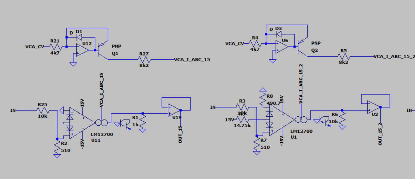
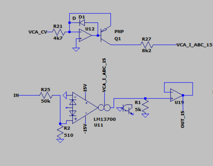
As a first model I used the Xonik VCA.

Xonik VCA

I first calibrated the circuit for unity gain at 5VCV, 15V supply, then updated it for 12V by replacing the diode bias resistor and doing slight changes to centering. (Actually, I made the 12V first then calculated a new diode bias resistor by first finding I_d as 11.3V / 12k = 0.942mA, then finding a new resistor as 14.3k / 0.942mA = 15.18k. The voltage across the resistor is said to be one diode drop away from the supply voltage).


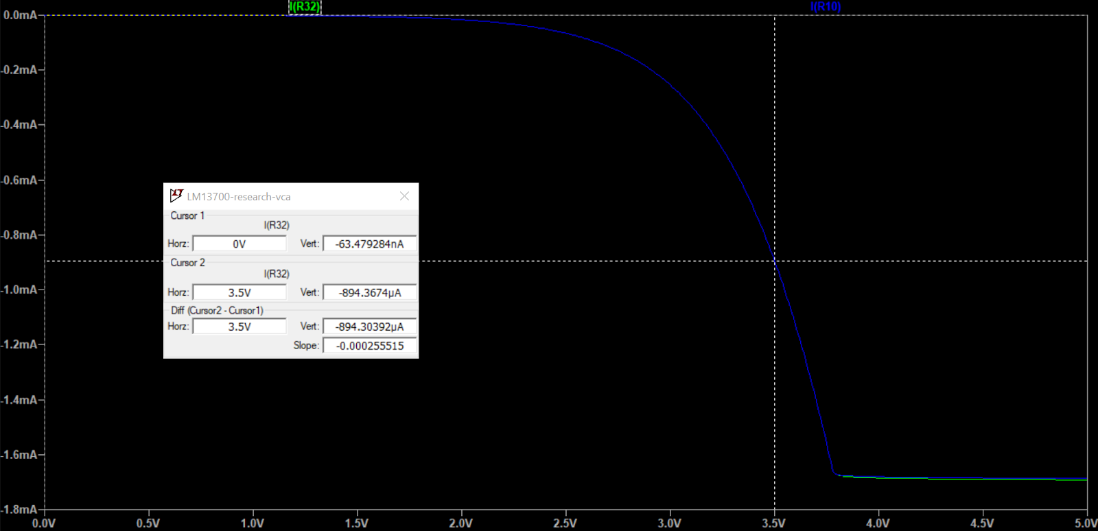
The output is also almost the same, with max output of the 12V being 0.98V instead of 1V:


I_abc for both 12 and 15V are exactly the same:


The voltages around the R_abc however, are very different as V_abc changes.


V_abc - these are fairly constant but drops abruptly when CV gets very small (the simulation used a resolution of 0.1mV, in reality the dropoff is even closer to 0VCV.


By manually tweaking R_d I was able to get an exact match with unity gain for both voltages. The R_d for 15V is slightly lower than expected. Perhaps a different value than 0.7 for diode drop is used in the simulator?


Here are updated measurements.

CV inputs

CV Supply Icv (=-I emm) I base Iabc Vabc V coll V base
0V12V0V0V0A-11.29-11.29V46.9nV
0V15V0V0V0A-14.27V-14.27V46.9nV
0.1V12V-21.7uA-224nA-22.4uA-10.47V-10.28V-675.9mV
0.1V15V-21.7uA-224nA-22.4uA-13.47V-13.28V-675.9mV
5V12V-1.064mA-10.5uA-1.053mA-10.26V-1.62V-775.6mV
5V15V-1.064mA-14.3uA-1.053mA-13.26V-4.63V-775.6mV

I've added an additional step at CV=0.1V, as the voltages around R_abc abruptly drop below this. This step shows that V_abc is fairly constant and not too far from the ideal supply-1.4V. 

So, what can we see from this? The only thing that changes when we switch supply (after replacing with updated R_d) is V_abc (which in turn changes V_coll). I_abc vs gain stays the same.

They also stay the same even if I_d changes.

Signal voltages

  • input is -5 to 5V.
  • CV is 5V
  • +in is connected to input through a 27k resistor and has a 510R to gnd
  • bias input is connected to 12/15V through 12k/14.75k resistor
  • Output is to gnd via 28.7k resistor, buffered.

Supply +in -in bias I out (to gnd) V out
12V 175mV to 275mV

(191.7uA to -175uA in 27k, 343uA to 539uA in 510R, -535uA to -365uA into +in)
184.5mV to 265mV

(373uA to 536uA)
1.03 to 1.12V

(-914.5uA to -907uA)
176.1uA to -174.8uAV out: -5.05 to +5.02
15V183mV to 283mV

(191.9uA to -174.7uA in 27k, 358.5uA to 554.5uA in 510R, -550uA to -380uA into +in)
191.9mV to 272.7mV
(391uA to 556uA)
1.04 to 1.13V

(-946.8uA to -940.7uA)
172.3 to -172.2uAV out: -4.95 to +4.94

These are practically identical, I assume that a bit of tweaking for R_d would make them exactly the same. Nice! That means that the same I_abc gives the same gain as long as I_d is tweaked due to the changes in supply voltages.

Juno expo converter

My juno expo converter is made to go to max, so it flatlines when CV > 3.5V. With adaptions between 12V and 15V (offset resistor and reference current resistor) they track the CV exactly the same, but the 15V version goes slightly higher.

15V and 12V expo circuits (VCA linear control circuit is still present but not used)

Both flatline when CV is high enough but 15V goes further


Voltages around R_abc are different, as expected. I've reduced CV to 0-3.5V to stay within operating range

V_abc is still fairly constant, with about 0.5V variation

V_coll

Again, as long as I_abc stays the same, the output stays the same. The expo converter generates the same I_abc as long as reference current and offset voltages are adjusted (and we stay within a range where voltages around R_abc can change enough to generate I_abc).

But we can do more! If we replace the 8.2k R_abc with a 6.4k, we allow a larger current through it with the same voltage. Then we get the exact same range as with 15V!


I_abc are now equal for both 12V and 15V

Outputs are equal too

In other words, we could probably do the same for the VCA to get the same range there as well. Turns out, we can:

Xonik VCA again


Going back to the version from my failed post, which uses this circuit:


and has this output:


If we just replace the 8.2k R_abc resistor with 6.4k, it works as it should:


Gain without I_d

First, I tried a version of the circuit with and without I_d


Two versions of the 15V circuit, tuned to be approximately the same

Signal input is -1 to +1V. From this plot it is quite clear that the one without I_d is not linear across the signal range:

The I_d version is completely linear whereas the non-I_d version is heavily distorted.


Increasing the input resistor and thus get a smaller differential input gives us a much more linear result:


In the datasheet, gain without I_d looks like it is not depending on supply voltage at all. Here is a plot of a 15V and a 12V version:

12V and 15V versions are very similar (but not 100%)

I retried with a smaller input resistor, 30k. Here is the input and output voltages, you can juuust see that the output is not entirely linear:

Voltage at positive input

Voltage at output, it is slightly curved downwards for the first 50% and then upwards for the rest.

As is expected from the datasheet, when not using a diode biasing current, the input must be attenuated a lot more to keep the gain linear across the signal range.


Gain measured vs calculated


For the version without I_d

Gain is expected to be:

I_out = V_in * I_abc * q / 2kT

where 

T = 283.15K (for 25C)
k = 1.38*10^-23 (Boltzmann constant)
q = 1.602*10^-19 (electron charge)

I_out = V_in * 19.47 * I_abc

(for T=300, gain is 19.3 * I_abc, which is almost exactly what is used in 8.3.3 and 8.3.4 in the datasheet).


This gives us for the 50k input version:

V_in+ is -11.18mV to 8.56mV, diff is 19.75mV
V_in- is -1.4959mV to -1.059mV, diff is 0,4369
V_in is -9.69mV to 9.62mV, diff is 19.31

I_abc = -1.05mA

Expected out is

I_out = 0.01931V * 19.47 * 0.00105A = -392.3uA


Measured output current

I_out = 213.13uA -149.72uA, diff is -362.85uA

The output current is independent of the R_out resistor, it only sets the output voltage.

This is fairly close to what the gain formula predicted, which is good.

However, I still have NO clue as to how I can find V_in+, V_in- or the differential voltage V_in. Without the last one this formula seems useless.

The same goes for the "missing gain formula" for the version with I_d. It needs the current in the input resistor, but how do I get that when I don't know the voltage at V_in+?

Closer measurements and useful V_in

UPDATE: After doing the version with I_d, and the email from Iain described below, I did some further simulation of the circuit. This time with both input offset resistors to ground in place. (I think the results would be close even without the negative one, the output would just be less centered).


Since the formula for I_out depends on the differential voltage, we cannot assume that the whole voltage drop is across the input resistor. 

However, the voltage at the negative terminal is much smaller the positive terminal, so we can choose to ignore it. We can also ignore the effect of the input transistor on the resistor divider formed by the input resistor and the resistor to ground. This means that an approximation of the differential voltage is

V_diff = V_in * R_g / (R_g + R_in)

where R_g is the resistor to ground.

When using the simulated differential voltage in the calculation, we get within 12-13% of the measured output value (for 500R resistors to gnd). Using the voltage divider voltage the error is 14-15%. I say that is plenty good enough :)

PS: The output current is not centered around 0A, this can be solved by either biasing or using a cap on the output.

1V sinewave input vs current output. Output is not centered. Using R_in=200k and R_g=1000


Simulated and calculated results.

PPS: The input voltages are not centered around 0V. To compensate for this, all voltage and current measurements in the spreadsheet above are the difference between the results for -1 and +1V input. Ideally, they should have been the averages, now they are twice that, which is why I've put 2x in all the columns. The formula still holds though.

With and without resistor from IN- to ground. Without (blue) the output has a larger DC component


For the version with I_d

Now, I wanted to see how much off the "missing formula" was and how it worked with the simulated results, so I did a lot of measurements using 250, 500 and 1000R resistors to ground, and 12.5k, 25k, 50k and 100k input resistors. I also tried both 12V and 15V supplies but they turned out the same.

I also wrote Iain Sharp and asked how he calculated I_g. He very kindly answered me almost immediately (thanks again Iain!), and the main takeaway from his long and detailed answer was that since the input voltage drop is so large compared to the DC offset at the input, I_g can be approximated as V_in / R_in. Nice!

(In general, Iain Sharp confirmed my suspicion that no one really knows exactly how the LM13700 works and everyone just experiment to get the wanted results. Incidentally, he read the first part of this post and got very worried that I do such detailed simulations without actually breadboarding anything as simulations are not the real deal. I will definitely test stuff in real life).

Anyhow, here is a table that includes both the measured voltages and currents, the expected output voltage using the formula but with the measured I_g, and the expected output using the formula with I_g as V_in/R_in:


All measured numbers are the difference between the results of -1 and 1V inputs, as I have not AC coupled anything. This means everything is double, which is quite confusing I guess. But the results are still valid.

There are a lot of numbers here, but the most interesting are:
- For the "standard" 500R resistors, the error is around 16-17%.
- There is only about 0.5 to 3 percentage points difference between using the simulated I_g vs the V_in/R_in one. A bit worse for the 1000R resistors and better for 250R.
- The simulated I_g makes the error constant as long as the resistors to gnd don't change.

A better I_g

Now. I had a look at what V+ voltage to expect if using a resistor voltage divider and ignoring that the center is connected to a transistor and a diode.

Interestingly, the result is almost exactly twice what we get when measuring. If we wanted to get a slightly better approximation for I_g (and one with a consistent error as we change the input resistor), we could use

V+ = V_in * R_offs/(2*(R_in-R_offs))

I_g = (V_in - V+) / R_in

where R_offs is the resistor from V+ to ground.

We still have a bigger problem with the formula though, so it probably isn't worth it. Just find an approximate output and simulate/measure your way to the correct values!

Other things to consider

The output in the version without I_d is not centered around 0, that is probably why there is a trimmer in the output VCA of the Juno filter, to add a DC component

Also, perhaps the filter does not use linearising diodes on the VCA as that allows a soft distortion similar to the non-linearity described above when the filter is overdriven.

DC operating point


The voltage input (base of the transistor) is not at 0 when the input voltage is removed, in other words, the input voltage at that point is centered around something else. If you need to find this, Iain Sharp had a nice way of thinking about it:


If you remove the input, you have two equal circuits around the differential transistors. 

In one leg, you have D1 and R1, in the other D2 and R2. 

Assuming R1 = R2, I_d is split equally between the two legs. We can also choose to ignore I_base as it is much smaller than I_d.

To get to ground, I_d must pass through R3 and the parallel equivalent of R1 and R2. Since R1 = R2, R1 || R2 is simply R1 / 2.

The combined voltage drop across the resistors is V_supply+ minus one diode voltage drop (roughly 0.7V) across the diode*. That gives us the formula for I_d:

I_d = (V_supply+ - 0.7V) / (R3 + 0.5 * R1)

Since I_d = I_R1 + I_R2, and I_R1 = I_R2, I_R1 is simply 0.5 * I_d

We can now find the voltage at the transistor base:

V_b = R1 * I_R1 = 0.5 * R1 * I_d = R1 * (V_supply+ - 0.7V) / (2 * (R3 + 0.5 R1)) 

V_b = R1 * (Vsupply+ - 0.7V) / (2R3 + R1)

* For the voltage drop I've assumed that 'reordering' the resistors and diodes so that it's R3 -> R1  || R2 -> D[1,2] and then calculated the equivalent resistance. I think this is ok but not 100% sure of it).


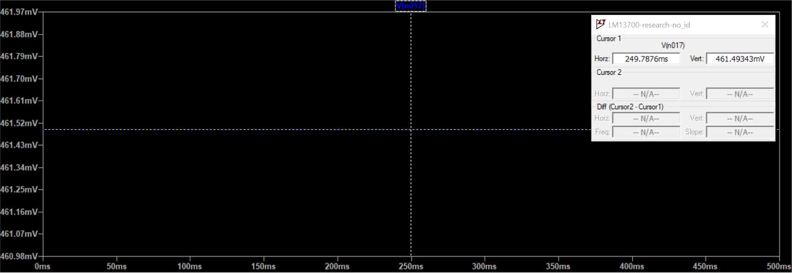
Tested circuit, input is +/-1V sine wave


Input at V_b, centered around 452mV


Circuit with input and R25 removed, shows 462mV DC offset

Measurements and calculations - for all lines with a value (100k, 50k, 25k) the input was connected to gnd. For the "no input" lines, input and R25 was removed. V+ calc is within 0.01V of measured value

Value at start of header lines is R1,R2.