Saturday, September 9, 2023

Replacing the door seal on a Miele W1 washing machine

Not exactly a synth thing, but something that definitely needs to be documented. My machine is a WKR771 (WKR771WPS), but the same instructions apply to a lot of Miele models

The seal on my 5.5 year old washing machine broke two weeks ago, leading to the fun situation where the machine filled the towel drawers below with water and leaving us with no washing machine just as our youngest had stopped wearing diapers, meaning A LOT of dirty clothes. 

Today the new seal arrived from Brøndum Elektro (a danish dealer that also sells to Norway). It took a long time, but their price was NOK 630, the only other supplier charged NOK 2300,- (about USD210 at the moment).

Now, to prepare myself I searched the net for how to replace the seal. I found several videos but none covered everything:

https://www.youtube.com/watch?v=6K375JeWVsw

https://www.youtube.com/watch?v=GLk8lucsmH0

https://www.youtube.com/watch?v=mi_znjVSoHk&t=34s

https://www.youtube.com/watch?v=j4IPS0wgc74


Uninstalling the old seal

Here is what I had to do:

Remove the top lid

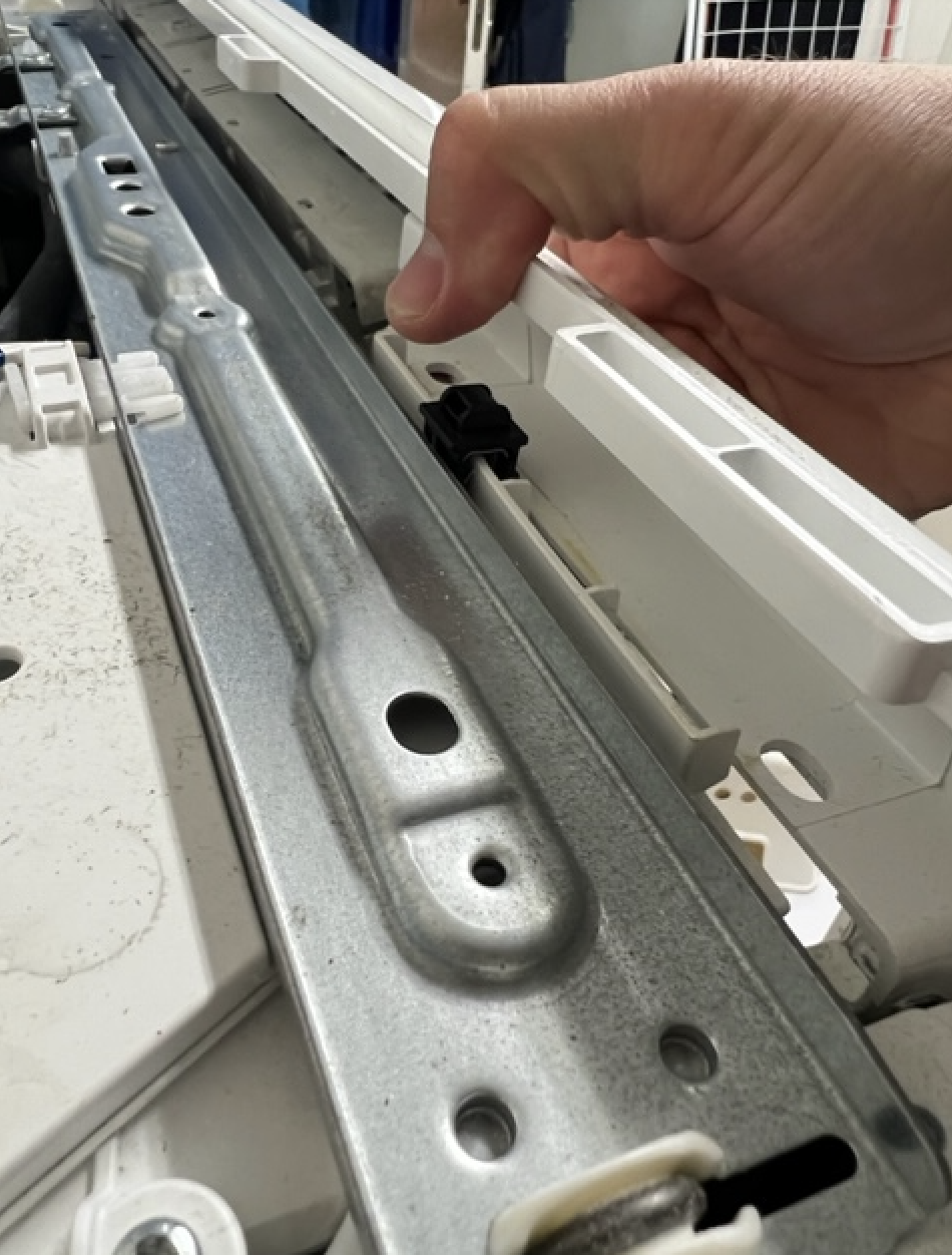
First of all, you need to remove the front panel completely. To do this, start by opening the two small plastic lids on each side covering the screws. I did scratch the lids but it doesn't matter to me as they cannot be seen anyway.


Unscrew the two screws. You can now lift the top lid in front. Lift it all the way up and it can easily be removed.

Remove the display/key panel

Next, remove the soap dispenser, and carefully pull forward on both sides of the plastic that holds the display and keys. Then pull everything up. The wires to the keys/display are a bit short but I managed to put the whole assembly on top of the washer without detaching the wires.


Detach the seal from the front 

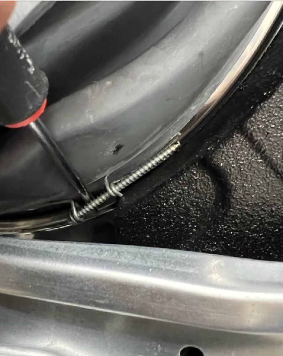
The seal is held in place by a steel wire with a spring on it. On my machine the spring is on the right side, by the door hinge, where the seal has a groove for it.


Use a flat head screwdriver to gently lift the spring. Once it is off, pull the seal lose.

Detach the front

The front is held in place by five screws: Two on the door latch, two on top and one large one below the center of the door.


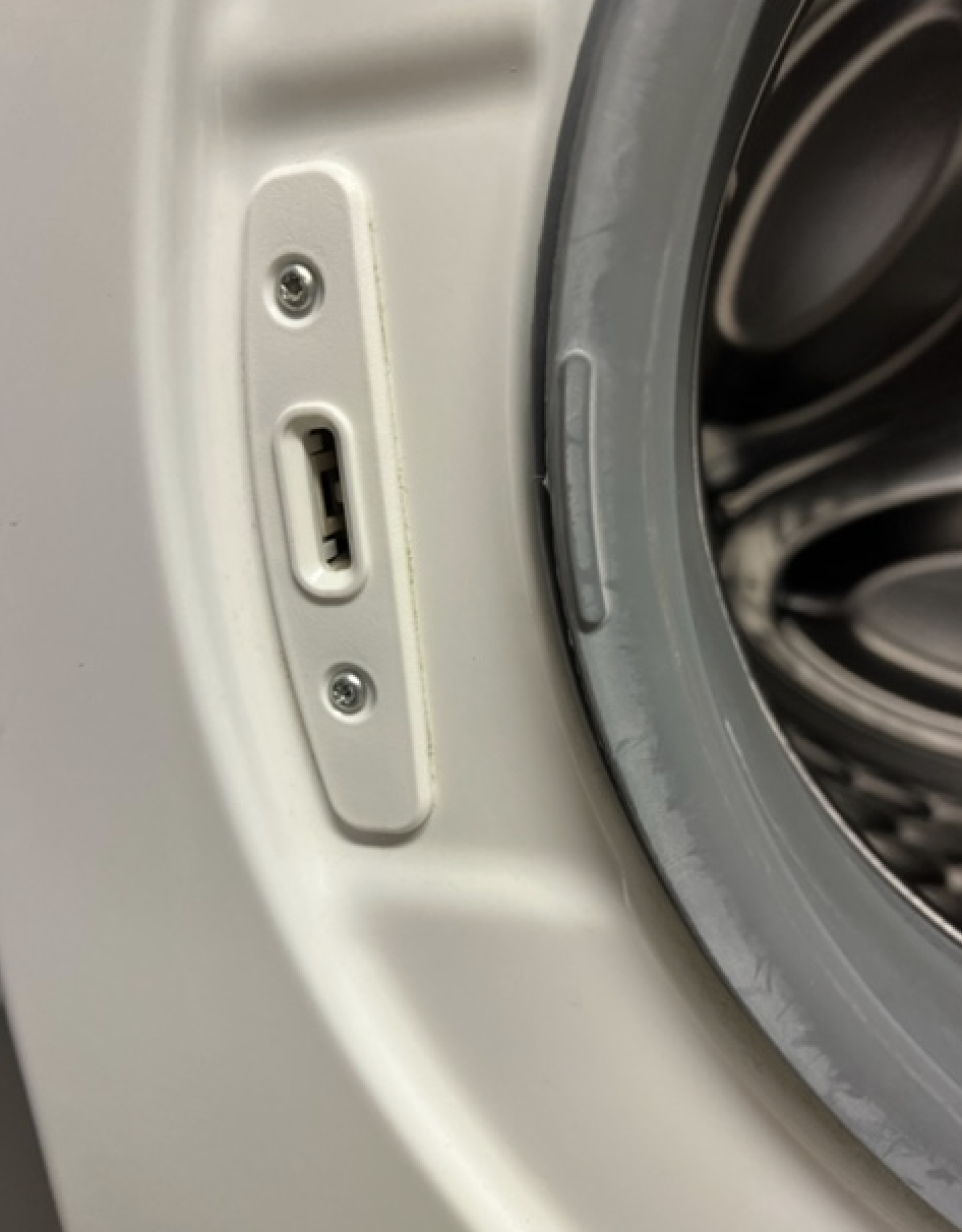


Now, find a T30 and a T20 screwdriver (you use the T20 for everything except the large one). Start by unscrewing the door latch, then the big one and finally the two on top. Once the last screw is removed, the front is lose and will fall forward. Fortunately, it is stopped by two plastic latches. To release these, push them down. You should now be able to lift off the front.


Remove the hoses and lights from the seal

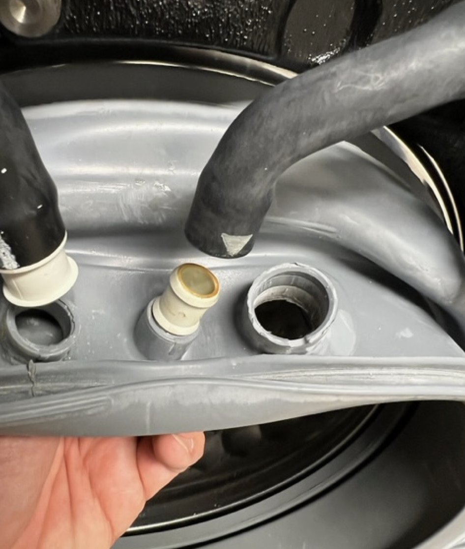
There are two hoses and one light on top of the seal. The left hose can be removed with the white plastic still attached. The center hose must be disconnected from the white plastic as it is too big to go through the hole. Finally, the light can be pushed from below to detach it.


Remove the left hose with the white plastic still attached

Detach the center hose from the white plastic


The white plastic will be reused

Push from below


Release the seal from the inner ring

Finally, you need to release the seal from the machine core. It is attached using a second steel wire, but this time it is tightened by a T20 screw. On my machine this can be reached from below using a long screw driver, and was fairly easy to unscrew. Make a note of how tight it was fastened to make reattaching it easier.
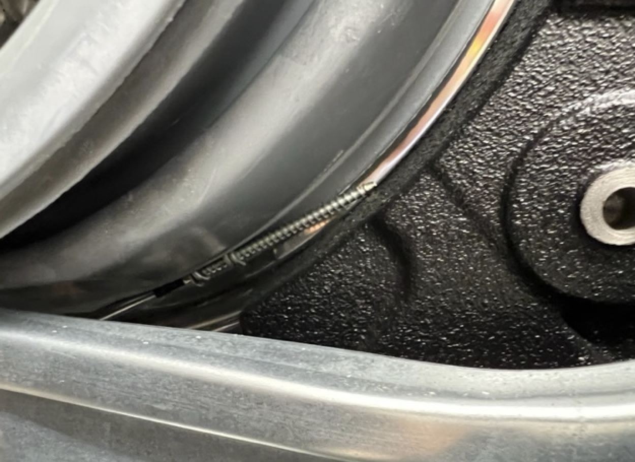

The T20 screw should be reachable from below


Gently pry loose the wire.


One problem I had was that even if I unscrewed the screw, the wire did not pull apart very much. Just pry it loose using a flat head screwdriver.

Remove the seal.

It took a bit of force to remove the seal, but I just started at the side with the screw and worked by way around.


Phew - at this point I started sweating - removing the part wasn't that hard, but I was quite nervous about putting the new back on.


Installing the new seal

Attach the wire to the new seal

Looking at the wire, I realised that I could slide it further apart after removal. I unscrewed the screw even further, so the wire slid easily over the new seal.


Align the seal

This is the single most important thing. You need to make sure the draining holes are at the bottom center and that the holes on top align with the hoses and light. It is nearly impossible to move the seal after you've started putting this on so do it right the first time.

On some of the other videos they made a point of aligning the drainage holes at the bottom of the seal with holes in the inner ring. My machine does not have these holes in the inner ring, yet it is still important to make sure the holes are at the very bottom or water will collect at this point.

Fold the seal over the edge of the inner ring

This was actually much easier than I anticipated. The ring goes into a quite deep groove in the seal, so I just worked my way around, putting everything in place. Make sure the steel wire stays on the outside of the rear flange of the seal all the way. Also, make sure to align the tightening screw so that you can reach it from below.

Make sure the screw is reachable from the bottom


Tighten the steel wire

Just screw the screw until it is as tight as it originally was. This went very smooth in my case.

Reattach the hoses

Putt back the two hoses and the light, make sure that the plastic parts are inserted all the way.

Attach the front panel

The front panel rests on two small white plastic parts. Align those with holes in the bottom metal of the front and gently push the front in place. Attach the two screws on top, the door latch and the big one below the door.


Attach the control panel

The panel slides down and is then pushed backwards until it snaps in place

Attach the seal to the front panel

This was way harder than I thought, but I ended up attaching the seal all the way around without the steel wire - as with the inner ring, I worked my way around while keeping an eye on the first point to make sure it didn't start slipping. I had to do this a few times before it snapped properly in place, but once it was on it stayed where it should


Attach the steel wire

This turned out to be a bit of a nightmare. Once again, you need to align the spring properly for it to fit in the groove by the door hinge.


I started on the left side and attached the top, then worked my way to the bottom while still holding the top in place, and pulling the spring apart slightly. It gets really tight and the wire starts dragging the seal away from the edge. I did at least five tried before I finally managed to get it on with a little help from a flat head screwdriver again (just make sure you don't ruin the seal). Make sure the whole seal looks even, I had to lift the spring a bit to release some parts that were stuck under the wire.


Reattach the lid

I tested the machine prior to this, just in case. The lid reattaches by placing it into two holes in the rear, then closing the front. Screw in the screws and pop in the lids. 


Congratulations!

Monday, September 4, 2023

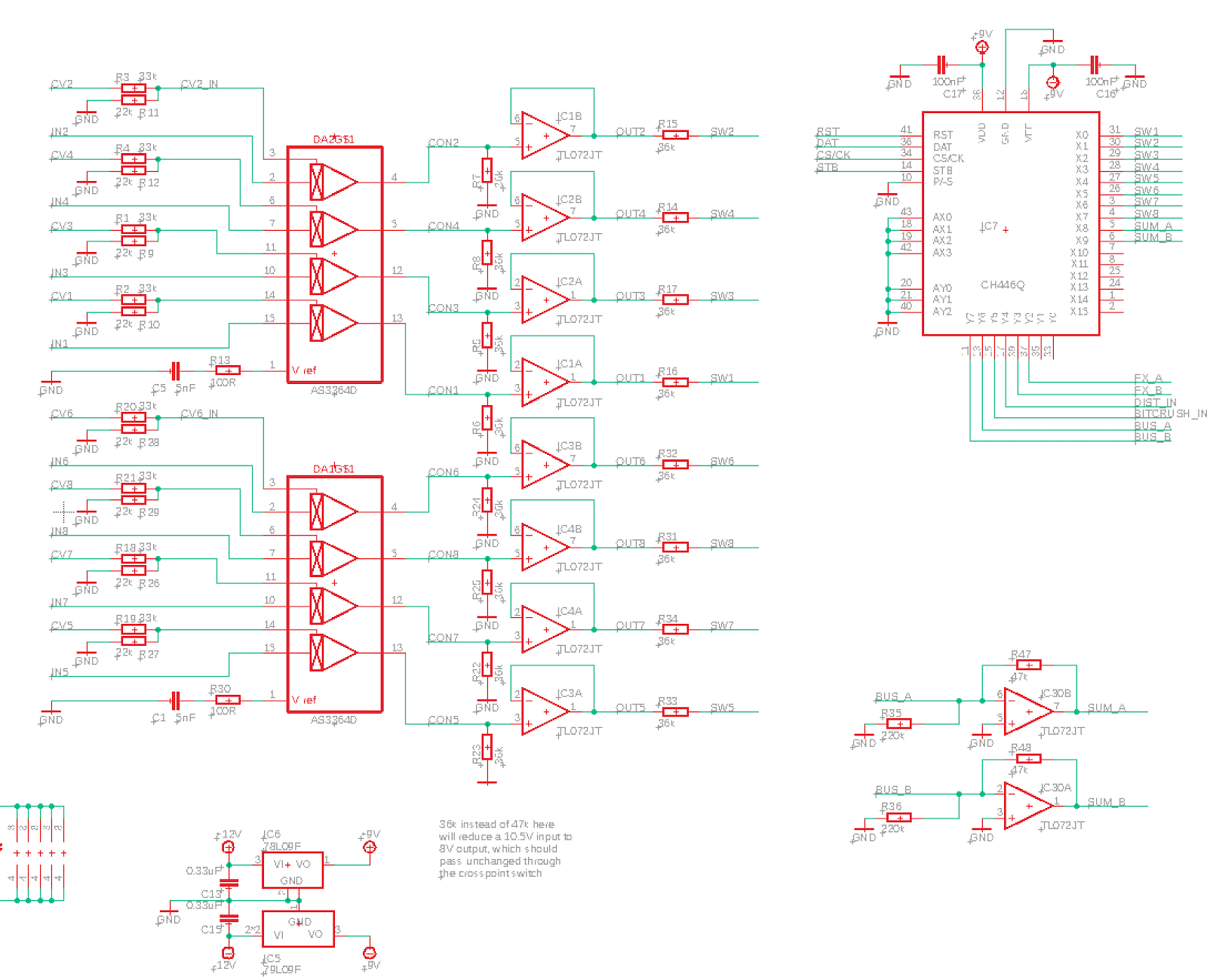
DG412 mixer vs ch446Q

I've breadboarded a DG412 based mixer to compare it to the CH446Q one.

To make things simpler, I've only breadboarded four inputs and two outputs, with two DG412/413 chips - this is half of everything on the CH446Q board (if we include the output mixer for the two FX channels, which I did when measuring current consumption on the CH446Q.

The biggest difference here, except for the size, is that the DG412 has parallel control inputs (i.e. one signal per switch) and the CH446Q uses SPI-ish. Thus, to compare the power consumption I should really add whatever current a 16 channel i2c port expander uses.

Anyway.

Current consumption

+12V: 12.3mA (24.6mA for full circuit)

-12V: 12.3mA (24.6mA for full circuit)

This is very interesting! If one ignores the fact that the negative current consumption of the CH446Q was very high for one device, this is exactly the same as the CH446Q board. The port expander (PCA9539) has a negligible supply current (200uA).    


Bleed through


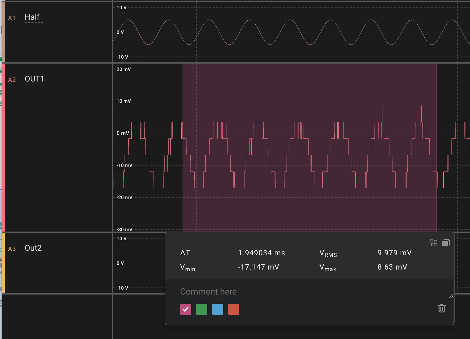
Average bleed through is +/-13mV for a +/-10V input.

As with the CH446Q, the switch sees the current from a +/-5V signal, and the output is +/-5V. To compare this with the CH446Q we need to multiply with 1.5 to get the +/-7.5V we have at the outputs, giving us a +/-20mV bleed through. This gives us -51dB, which is definitely not better than the CH446Q. Now, the datasheet says that off isolation should be -68dB which is quite a bit better than this so I'm not sure where the leakage is. 

With TWO inputs of the same signal going to a mixing op amp, I see +/-23mV (=+/-35mV) leakage, which is to be expected I guess, as both switches leak. 

I cannot see any leakage to the neighbouring channel so no visible crosstalk, just bleed through.

Conclusion
The performance of the DG412 vs CH446Q is not that different, neither in terms of current consumption or bleed/crosstalk. What I choose to use comes down to two things:
- board space - The DG412 solution takes up much more space if using DIL chips)
- serviceability - The CH446Q is extremely custom and may be hard to get at a reasonable price whereas the DG412 is available from several suppliers and I have a lot in stock. Also, it is possible to replace a single DG412, if the CH446Q breaks I must replace a whole bus board.

Sunday, September 3, 2023

CH446Q/X testing

Initial testing

 +/-9V supplies are ok but chip gets hot.

3.3V logic ok

SPI bus at 32MHz ok, at 35MHz it drops commands.


Weird way of working

Need to send reset to get chip going, probably syncing SPI bus etc

First send address

Then set MOSI pin to the state we want (which requires us to disable the SPI bus)

Turn on and off strobe for 10ns.


Tested

Mixing two inputs

Signal 3Hz to 35kHz tested ok


Inputs:

Input 1 (internal 0 and 1) ok

Input 2 (internal 2 and 3) ok

Input 3 (internal 4 and 5) ok

Input 4 (internal 6 and 7) ok

Input 5 (internal 8 and 9) ok

Input 6 (internal 10 and 11) ok

Input 7 (internal 12 and 13) ok

Input 8 (internal 14 and 15) ok


Outputs:

Sum A and B ok sums inputs correctly

FX A and B ok, sums inputs correctly


Crosstalk

Visible crosstalk between FX A and B, particularly when input is not connected to anything. Lowerst when input (in 8/internal 15 during testing) is connected to Bus A, more when connected to Bus B

Output til Bus A:

- Crosstalk on FX A: -9.7 to 37.5mV, avg 23.6mV

- Crosstalk on FX B: 1.49 to 22.4mV, avg 10.5mV

Output til Bus B:

- Crosstalk on FX A: -35.9 to 69mV, avg 52.45

- Crosstalk on FX B: -3.7 to 22.4mV, avg 13.2

Input not connected to output:

- Crosstalk on FX A: -56.9 to 90mV, avg 73.45

- Crosstalk on FX B: -19.4 to 38mV, avg 28.7


Crosstalk pĂ¥ Bus A/Bus B:

When everything is off

- Bus A: -22.3mV to 13.8mV, avg 18.1mV

- Bus B: -9.5 to 11.3mV, avg 10.4mV

When other bus is on

- Bus A: -12.0 to 3.5mV, avg 7.75mV

- Bus B: 9.45 to 11.3mV, avg 10.4mV


When output is to FX A and FX B:

Crosstalk on bus A and B looks a bit higher

Tried switching Bus A to input 1 with 33k to gnd, no improvement.


NB: Resolution of the logic probes is around 6mV

If one assumes an input of 2.5V, the highest crosstalk is (90--57)/2=74mV, so signal to crosstalk is attenuated 33 times (i.e. 3% of input). This corresponds to -30dB. Not impressive I think?

I cannot find any info about crosstalk in the CH446Q datasheet, but the MT8816 (which is sort of compatible) has a crosstalk between -45dB (for 2Vpp sine with freq 10MHz) and -85dB (for 10kHz)

-85dB corresponds to a V_in/V_crosstalk ratio of 0.0001

That would mean an input of +/-2.5V would result in crosstalk of 0.25mV

-45dB corresponds to a V_in/V_crosstalk ratio of 0.0056

That would mean an input of +/-2.5V would result in crosstalk of 14mV

This is not that far off from what we see when the input goes to one of the output busses. The max crosstalk is when the input is just blocked. 

PS: In the tests above we always have TWO input signals, as every input is split in two. That means that even when one is passed, the other one is blocked. And when both are blocked, we get the same signal contributing to crosstalk twice. 

Next to test:

- Is crosstalk the same if power is +/-5V as +/-9V?

- Is crosstalk reduced when we only have ONE copy of a signal?

- What is the crosstalk if we sink all non-used inputs to an output? 

- Is the crosstalk the same if I switch to a new mixer board that was not heated as much by accident (!).

- What is the crosstalk on a DG412 (said to be -85dB, with -65dB offness to switch

- And not least, am I able to hear 75mV crosstalk at all? Especially when whatever it passes will be sent to the other filter and probably in some form to the output.


CH446X on breadboard

Testing with direct input of 3.5V, dropped through a 47k resistor before the switch, which gives the same current through the switch as the 2.5V/33k input of the bus mixer circuit.

Switching between Y0 (pin 43) and Y3 (pin 42), connected to an inverting opamp (47k in feedback). 

Crosstalk

Only one input used, resistor before switch so 0 voltage at switch:

Y0: crosstalk is mostly 0.9-6.1mV (avg 2.6mV) with some jumps to as much as -4/16mV. 2.6mV/3600mV = -63dB, which is close to the offness of the DF412 switches)

Y3: crosstalk is mostly 11-16-mV (avg 2.5mV) with some jumps to as much as 0.7/32mV

Only one input used, resistor after switch so full voltage swing at switch:

This does not work at all! No idea why. 

Only one input used, 1.2k resistor before and 47k after switch, almost all of the voltage swing is across the switch:

Crosstalk is now -25mV to 53mV or avg 39mV


Now something is wrong: It seems that the chip locks up and is not able to start properly, supply lines are not +/-5V and it draws a LOT of current. I managed to get it started again once, but after moving around resistors it locked up again.

To test I removed all ground connections from X-inputs. I just read that I should have done the opposite: "CMOS switches and multiplexers are symmetrical devices; their signal input and output terminals are interchangeable, so unused ones should all be considered to be inputs, not outputs. Thus, they should all be grounded."

Also, read this: https://www.ti.com/lit/an/scda011/scda011.pdf?ts=1693203318955&ref_url=https%253A%252F%252Fwww.google.com%252F

I re-added the gnd connections on all unused X and Y inputs, but nothing works. I will order a socket and try with an unused CH446X. 

Second try, bus mixer

I went back and tried the bus mixer again. I didn't see as much crosstalk this time. Here we see input 0 going to output 2, 3 and 6 (FX A, FX B and SUM A) then pause for 200mS. For FX A and SUM A crosstalk is +/-6mV, while FX A has a crosstalk of +/-12mV.


Input is +/-10V going through a 33k/33k voltage divider so the bus mixer sees +/-5V at the input. This is amplified to +/-7.3V at the outputs, so any crosstalk is in relation to this. Right now, we see 6mV crosstalk on 7.3, which is around 61dB. That's ok I think.


Current consumption

The CH446Q and op amps on the mixer board runs rather hot, so I checked the current consumption without the AS3364 installed. The measurements include the op amp on the FX outputs which is external to the board. I got:

- 24mA on the 12V input

- 45-55mA on the -12V input (changing up and down. 45 when no output is on, 55 when one or more outputs are on).

A second mixer board, that has not had the output fix for bus wiring, and has never had any power issues, runs at around 23mA on the -12V input (as well as 24mA on the +12V input), which seems much more correct. Also, it doesn't fluctuate as much.

A TL07x op amp typically consumes 1.4mA. I have 8 of them, which should account for 11.2mA approx, leaving 12.8mA for the crosspoint switch, including some loss at the voltage regulators. It doesn't sound entirely unreasonable. I need to compare this to what DG412 uses.


Full bus mixer

I added two AS3364 quad vca chips and tested the control signals with 0 and 5V (though not anything in between). It worked flawlessly, though the output is perhaps +/- 0.2V below unity gain.

The current usage with two AS3364 is 37mA (+12V) and 55-69mA (-12V), so roughly 10mA more on each supply

Working program

#include <SPI.h>

#include "stdint.h"


#define PIN_CH446Q_STROBE 4

#define PIN_CH446Q_RESET 21


void setup() {

  pinMode(PIN_CH446Q_STROBE, OUTPUT);

  pinMode(PIN_CH446Q_RESET, OUTPUT);

  pinMode(11, OUTPUT);


  digitalWriteFast(PIN_CH446Q_STROBE, LOW);

  digitalWriteFast(PIN_CH446Q_RESET, LOW);

  delay(1);

  digitalWriteFast(PIN_CH446Q_RESET, HIGH);

  delay(1);

  digitalWriteFast(PIN_CH446Q_RESET, LOW);

}


void setSwitch(uint8_t in, uint8_t out, uint8_t on){

  uint8_t address = out * 16 + in;


  // We need to use begin and end to regain control of the pin

  // after the address is transfered, without this we cannot 

  // set the switch mode. 

  // 32MHz is the highest stable speed I was able to make work.

  SPI.begin();

  SPI.beginTransaction(SPISettings(32000000, MSBFIRST, SPI_MODE0)); 

  SPI.transfer(address);

  SPI.end();


  // After writing the address, we need to set the MOSI pin to the 

  // wanted state of the switch, 0 for off and 1 for on, before

  // strobing the strobe.

  pinMode(11, OUTPUT);

  digitalWriteFast(11, on);


  // Strobe makes the switch... switch.

  digitalWriteFast(PIN_CH446Q_STROBE, HIGH);

  delayNanoseconds(20);

  digitalWriteFast(PIN_CH446Q_STROBE, LOW);

} 


void loop() {

  setSwitch(0, 6, 1);      

  delay(500);

  setSwitch(1, 6, 1);      

  delay(500);      

  setSwitch(0, 6, 0);      

  delay(500);

  setSwitch(1, 6, 0);      

  delay(500);

}

Friday, August 18, 2023

Output phase, SVF Cell 1 and 2

Cell 1


LP, BP and HP are in phase with the filter input (which is NOT the cell input, but IS the summing point for feedback).

Notch, however, is reverse before and after the notch point. This means it will not work with feedback. I address this further down in this post.

Allpass is in phase before and after the cutoff frequency, and 180 degrees off at the cutoff frequency. I am not sure if this is wrong and has to be corrected, I need to check the expected behaviour, though I believe that adding AP and dry should give a notch, which is what would happen here as the 180 degrees off at cutoff would cancel out the dry signal.

Cell 2

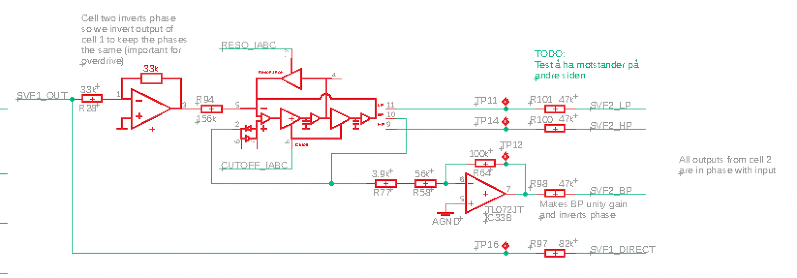
Cell 2, all outputs are in phase with input


The outputs of Cell 2 (as seen by the mux) is in phase with its input (Holds true for LP, BP and HP, and of course for the Cell 1 direct as this is the same as the input to Cell 2).

The op amp after the mux inverts the signal so the output phase of the filter is inverted. 


This affects both the output itself and the filter feedback. The output phase is selectable so that's taken care of there. The feedback on the other hand, is inverted back in the feedback VCA (positive input + inverting op amp).

Feedback VCA inverts signal

Alternative notch

Combining dry (inverted) and BP (unity gain) can give me notch without having to add another op amp (as described here: http://atosynth.blogspot.com/2019/01/jupiter-6-all-pass-filter.html)


Simulating this shows a big difference in the offness of the notch - green is LP + HP, red is dry + BP.


From the simulation, LP + HP results in a -1.2dB down to -36dB notch. Dry + BP results in -19.5dB.


Measured in my circuit I see approx +/-150mV for LP+HP, though it looks a bit noisy. Dry + BP is +/-375mV.


Also, gain when no notch is a little low:


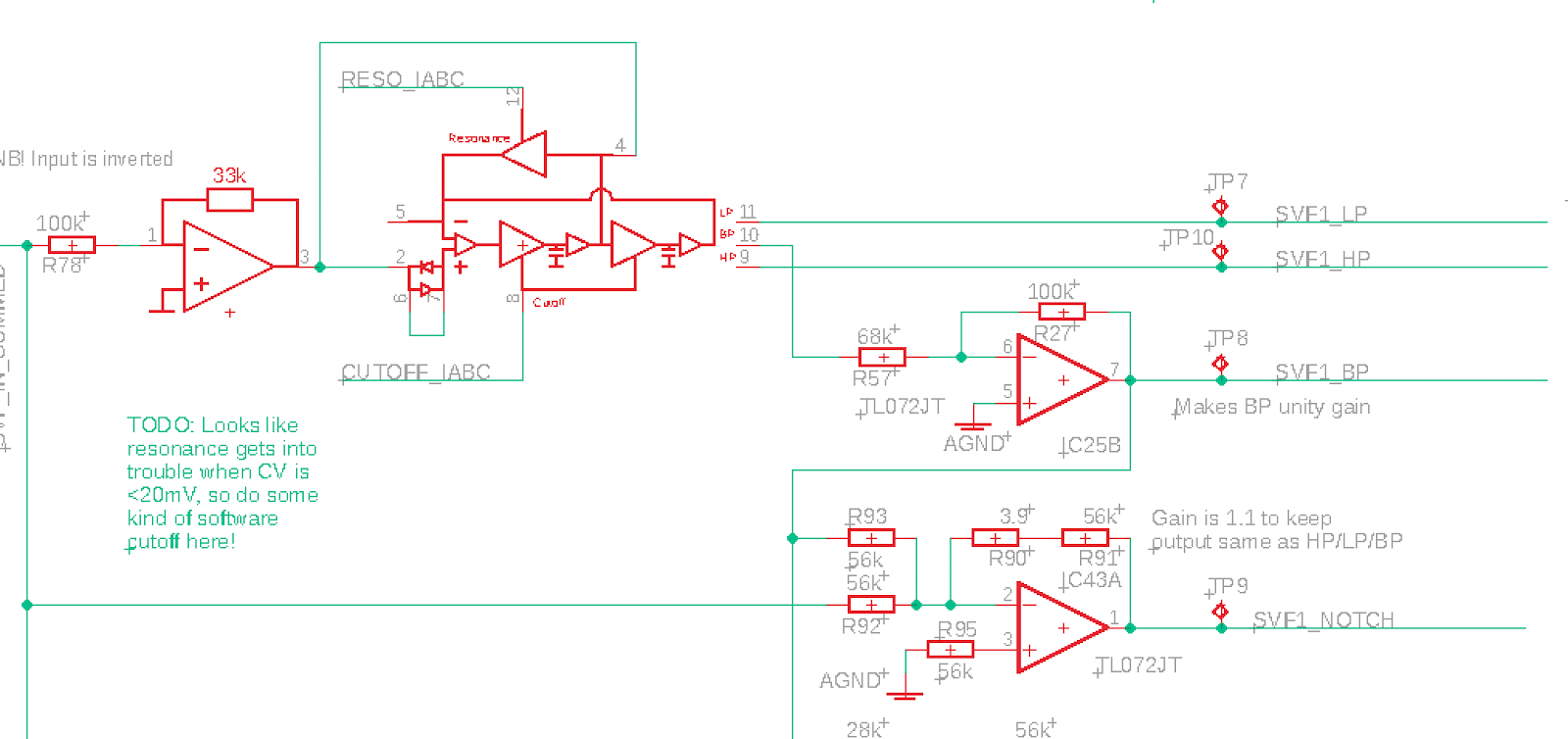
The output is +/-5V. To boost it to +/-5.5V which is the range of the other waveforms, we can use 56k + 3.9k in op amp feedback, making the gain 1.07

Here is the alternative notch circuit:


Thursday, August 10, 2023

Output levels, SVF Cell 1 & 2

Cell 1

I've measured the output levels of three different circuits for cell 1 of the SVF.

The results are fairly stable, within approx 0.05-0.1V between cells.

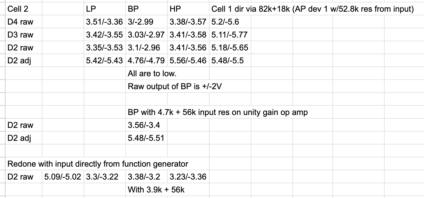
Output of LP, BP, HP and Notch are all around +/-5.5V when input is +/-5.0V. 

As I mix BP with input, and the output should be 2 x BP + Input, we have to reduce the input resistor for input to boost it from 5 to 5.5V approx. 

BP output is between +/-5.3 and +/-5.4 for all cards, so gain needs to be between 5.3/5 = 1.06 and 5.4/5 = 1.08 Experimentiation showed that using a 51k and 1.8k resistor in series, combined with the 56k feedback resistor, gave a good result. The calculated gain for this is 1.06.


Cell 2

I did the same for Cell 2, testing device 2, 3 and 4 against each other, and again they match fairly well.

Raw output is around +/-3.4V with a little offset. BP, however, was too low even after the 100k/67k boost and came out around +/-3V. After some experimenting I chose to replace the 67k resistor with 4.7k + 56k, which brought BP up to the same as the others.

The output after final amplification is +/-5.4 to 5.5V which is approx the same as from cell 1. Not sure if I should adjust this back to +/-5V, as the input is 5V, I guess unity gain is a nice feature so perhaps worth the extra work.


Monday, August 7, 2023

CMOS switches and current switching

After my previous post where I discovered that Douglas Self has some examples where he's switching mixer inputs at the op amp virtual ground, and after talking to the guy on Reddit that made me discover the CH446Q (ARabidSquid, Architeuthis Flux on Tindie), I decided to test it in practice.

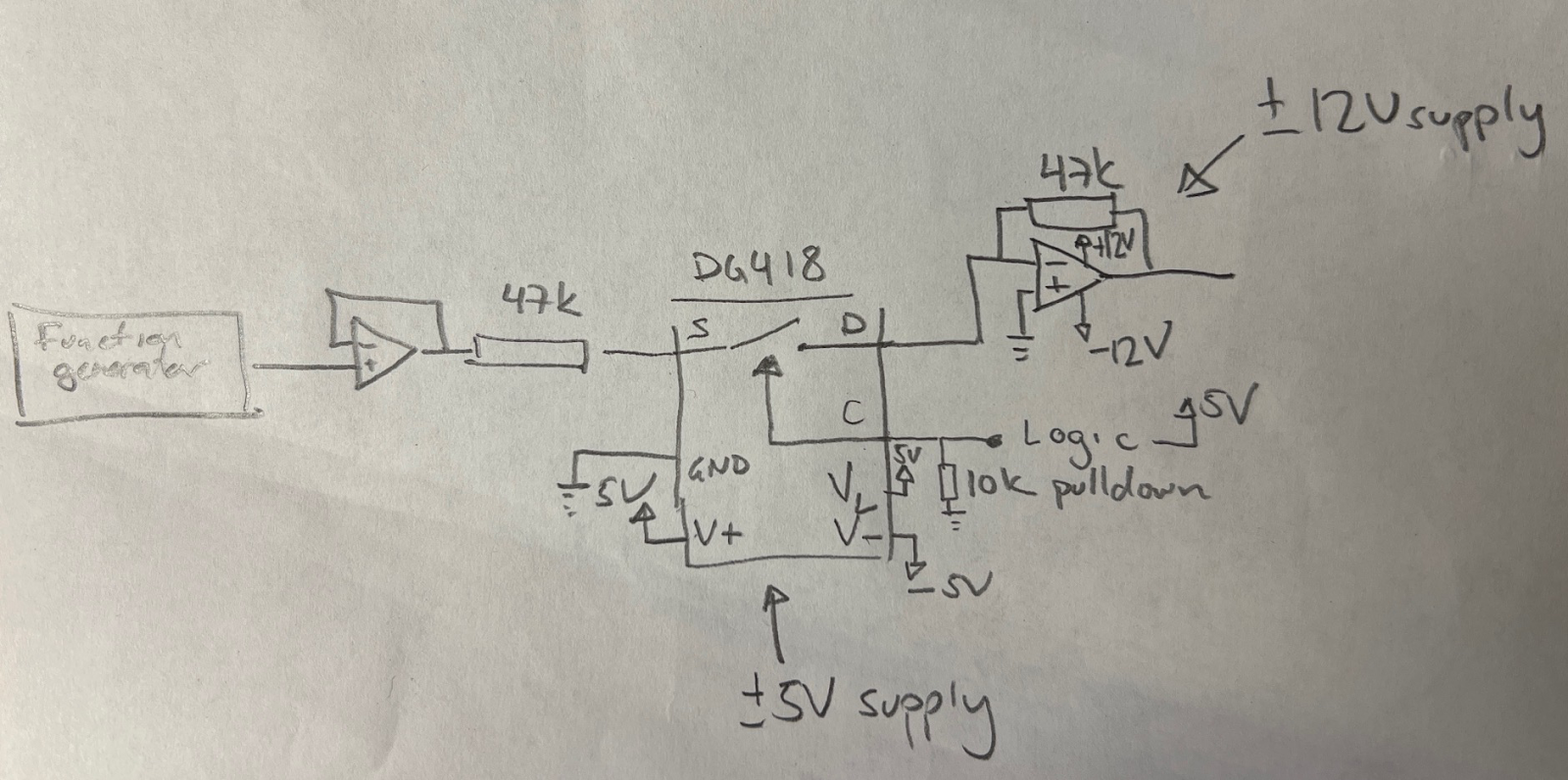
I hooked up a DG418 on a breadboard, and used an 78L05 and 79L05 to get a +/-5V supply for the DG418.

I then used a TL072 op amp with +/-12V supplies, with one op amp to buffer the input from the function generator and the second to "sum" (just invert really) the output from the switch, with a 47k negative feedback resistor. 

Version of circuit where input resistor is before the switch


I could now experiment with having the op amp input resistor BEFORE the switch (placing the switch at the virtual ground) or AFTER the switch

An initial test with a 10Vpp (+/-5V) signal showed that it worked in both configurations.

Resistor after the switch, 10Vpp

Resistor before the switch, 10Vpp


I then placed a 20Vpp signal on the version with the resistor after the switch. As expected, the switch clips the signal since it sees the full 20Vpp, but exactly how it clips is interesting. Measured at the input pin (i.e. the output of the buffer), the INPUT is clipped - the top is at 9.16V and the bottom at -5.85. I didn't expect it to be asymmetrical.

Resistor after the switch, 20Vpp. Output (and input) clips


Next up, I moved the resistor to before the input. The switch should now see no voltage swing (though a current passes through, +/-0.2mV at its peaks). This also worked as expected, the output is also 20Vpp (though inverted because of the op amp configuration).

Resistor before switch, 20Vpp passes nicely


This looked very promising. Next up was turning the switch OFF. 

Again, for the 10Vpp signal, it worked as it should for both variations.

Switch off, 10Vpp


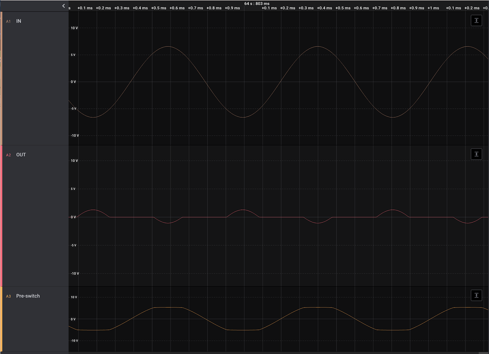
I then tried cranking up the signal for the variation with the resistor before the switch, but then "disaster" struck: Once the input signal got higher than the DG418's supplies, it started leaking! With a 13Vpp input, it blocked everything up to 10Vpp. The remaining, however, was passed through, giving the output small "bumps"! 

Resistor before switch, switch off, 13Vpp. Anything above approx 5.1V is passed, giving funny little bumps on the output.


When showing the result to ARabidSquid, he confirmed that this was how CMOS operate, it cannot block anything higher than it's supply voltages.

After seeing this result, I remembered that I read something similar yesterday - someone posted about a similar issue, where a current input made the switch leak when it was turned on. Someone suggested using an SPDT (or two switches in a crosspoint switch) to sink the current. This could be an option, to use a separate bus to sink all input signals that are not in use. However, I think I'd rather stay within the operating limits and keep my signals at 16Vpp max.

Sunday, August 6, 2023

Mix bus and channel muting

I'm designing a variation of my pre filter mixer using the CH446Q 8x16 crosspoint switch, and while doing so I started wondering if having the switch after the mix input resistor was a good thing or not. 

Douglas Self to the rescue, seems that switching directly to the virtual ground of the mixer summer is the way to go.

From "Self on Audio" by Douglas Self - Figure A seems to be the way to do things which is what I've done in my new design.

My mixer


Sunday, July 23, 2023

I don't understand how to use AP

Now that the AP is working properly on the JP6 filter, I'm trying to understand how to use it.

Most places say that you should mix it with the original signal, but when I do that I get exactly what I get from my notch:

Red: Notch. Blue: 50% AP + 50% Dry


Sunday, July 9, 2023

JP6 gain through cell 2

In the simulation, cell 2 outputs a +/- 2.6V signal when output from Cell 1 is 4V. This in turn arrives at the output as 3.1V and is overdriven to 4V with a nice rounded shape. 

Now, the output gain feedback resistor is 100k. Let's do some calculations.

LP and HP are tapped through 33k + 47k = 80k. That should give a gain of 1.25, which should give an output of 2.6 * 1.25 = 3.25.

The output of the BP requires a gain of 1.33 in cell1 in the simulation, and 1.5 on the breadboard, to be equal to the LP and HP outputs

That means a total gain of 1.25 * 1.33 = 1.66 (or 1.88 on the breadboard)

Thus, we need 100k / x = 1.66, x= 60k (or 53k for the breadboard).

For the direct output from cell 1, which is at 4V in the simulation, to get it to 3.1 requires a gain of 3.25/4 = 0.81, or a 125k input resistor. 

Now, wait a minute. Gain < 1 is generally not something we do, we usually do it by using a resistor divider. But let's not, let's rise the output level from 3.25 to 4 instead, meaning we only need unity gain for cell 1.

That gives us the input resistor for LP/HP as

gain = 4/2.6 = 1.54, R = 65k

and for BP

gain  = 1.33 * 1.54 = 2, R = 50k (and 1.5 * 1.54 = 2.3, r = 43.5)

Let's see what this does in the simulation:

Well, LP still looks good, at just a tad below 4V. Then, turning up overload to max fivces a slightly more distorted wave, but still cool, and with an amplitude of 5.1.

Now for another check, what happens with a 20Vpp signal. Does it distort?

It definitely does, but that's not because of the feedback, it's just how the circuit works.

We could get around this by using a 200k input resistor instead of a 100k, and then double the gain at the end of the circuit instead. We'll just have to try this to see how it affects both a 5V and 10V signal when doing distortion.

On breadboard

I tried sending a 5V signal through cell 2, and I get 3.23V on LP, 3.32V on HP and 2V on BP, meaning we need a gain around 1.6 for BP. 

To get all up to 5V at the output would require gains of
HP/LP: 5 / 3.23 = 1.54
BP: 5 / 2 = 2.5
and unity.

100k / 1.54 = 65k
100k / 2.5 = 40k

So a combination of 47k and 18k, and 22k and 18k is a good starting point.

Testing: 
LP: Near perfect 5V out
HP: Output is 5.2V, so a tiny bit too high
BP: Damn close to correct.


This means I will try the following for cell 2 in "production":
HP and LP: 47k +18k
BP: 22k + 18k
Direct: 82k + 18k

For cell 1 I will use 56k for everything, but BP is boosted by 1.5 using a 150k feedback and 100k input resistor


Next things to try on breadboard:
- overdrive
- no resistor pre-mux for cell 1
- swap cells to see if they behave similarly
- output vca.
- polaritites for output VCA and overdrive, see if we should modify cell circuit

See "Jupiter 6 filter - no VCA - 12V - JOVE trials -overdrive"


Saturday, July 8, 2023

JP6 All-pass - inverting BP

In my simulations and breadboarding I added an inverting op amp for the input to get AP. But what if we instead inverted BP? It is already 180 degrees off compared to HP and LP. 

I simulated this, and it looks like it works well. Instead of going from -360 to 0 degrees it goes from -180 to 180, which is just to say that the output is inverted compared to the input - just like HP and LP.

As I'm already planning on having an invert button/switch on the SVF this doesn't matter :-D 

It also saves me one opamp.

As for the opamp gain, to keep the gain at 1.48 (or 1.5, it probably doesnt matter too much) we can go with 100k input and 150k feedback, or 68k/100k.

I will try this now.

JP6 All-pass tested

I've breadboarded and tested the AP-filter from my all-pass simulation, version AP-C: https://atosynth.blogspot.com/2023/04/jp6-filter-allpass.html

It only required minor tweaks.

During testing, my BP outputs +/-3.5V and the HP/LP outputs +/-5.2V. I assume that BP is affected the same way HP/LP is by the resonance feedback, so adjusting feedback so that HP/LP are normally +/-5V probably also affects BP amplitude.

Anyway, to get AP we need to mix 2x BP with the inverted input. But the BP needs to be unity gain.

If we assume that unity gain is +/-5V when properly adjusted, it is 5.2 when HP/LP is 5.2. That means that to bring it up from 3.5V to 5.2V we need a gain of 1.48. The simulated circuit has a gain of 1.33 when using a 100k/33k combination. Replacing the 100k with 68k gives us the gain of 1.48 that we want. 

Here is a video of turning the cutoff CV knob, see how the phase changes.


The resulting circuit is like this:


PS: We need to sum everything BEFORE it reaches the filter as we need input both for AP and normal input. But this affects the polarity of the input and probably also the feedback circuit.

PPS: I am not sure how we can use AP/Phasing. Do we need to be able to pan wet/dry to different channels? Should this be an option anyway for filter outputs?


Update: Here is an alternative circuit, the AP output phase is 180 degrees different from the one above but it saves one op amp that can be used to sum stuff before the filter


Friday, July 7, 2023

New measurements with JOVE CV generation and working Cell 1 and 2

NB: R_abc is 10k instead of the 18k found in the JOVE circuit.

Resonance

I think the resonance looks quite good

Here are some quick measurements of the resonance voltages using the JOVE resonance circuit. This seems to give approxmiately unity gain for HP/LP and self resonance (could perhaps be a bit better).

Output of trimmer 1: -2.83V
Output of trimmer 2: -10.83V

Reso CV: 0V
Output CV mixer: 2.9V
Base voltage: -52mV

Reso CV: 5V
Output CV mixer: 7.94V
Base voltage: -10mV

Cutoff

The cutoff range seems too limited, but with this, a 50Hz wave has an amplitude of approx 130mVpp. At max, the HP filter lets a 1.5kHz wave through with 180mVpp. An 8k wave has approx 5Vpp amplitude.

Cutoff trimmer 1: -8.4V

Cutoff CV 0:
Output CV mixer: 998mV
Base voltage: 100mV

Cutoff CV 5:
Output CV mixer: -1.25V
Base voltage: -100mV

Polarities
LP output, Cell 1: inverted
BP output, Cell 1: normal
HP output, Cell 1: inverted

Amplitudes 
HLP Max: +/-5.25V
BP Max: +/-3.5V
HP Max: +/-5.25V

High frequency oscillations
The high frequency oscillations seen previously are completely gone (though I have not tested with higher CV), perhaps they were caused by the erroneous 3p filter cap

Thursday, July 6, 2023

JP6 filter oscillations and latch-up

I've had serious troubles with the JP6 filter since I started working on it again about a week ago.

- it latched up whenever the cutoff CV was > 1.5V
- it had severe high-frequency oscillations

Today, I finally got it working again (with the Jove CV generation circuits). Here are the three things I fixed:

- Cutoff and Resonance Iabc has to go to two cells, not only one (or they will be too large)
- I had messed up and used a 3pF instead of a 330pF cap
- And even after fixing that, I realised that the caps were probably not in contact with the connectors. I redid the wiring there and everything started working.

Back to the real testing!

Sunday, June 11, 2023

JP6 vs Jove revisited

As part of getting my JP6 filter working, I thought it would be a good idea to revisit the Jove JP6 filter (https://system80.net/product/jove/, https://github.com/minisystem/JOVE) to compare it to what I'm doing. It is especially interesting to see how the control signals differ, and what their ranges are.

The conclusion is that everything is very similar and my control signals cover the Jove signal ranges - but it is worth mentioning that the cutoff maxes out at around 23kHz on the Jove.

Here are my findings in detail:

Resonance

My simulation doc says the following about calibrating resonance CV:

Tune U30 until you get -125uA Reso I_abc per OTA (or to freq response is OK)

Tune U31 until you get -25uA or -4uA Reso I_abc per OTA (for similar response to 5 or 10V CV on the JP6)

Comparing to the Jove reso circuit, this is exactly what you get from trimmer extreme, -120uA to -4.2uA, so a range of -120uA to 0uA is what we want to be able to trim from software

In the following, the three lines correspond to min, center and max trimmer settings:

Jove resonance - voltage seen at expo converter input

Jove resonance 0-10V - I_abc in single 18k resistor


Jove resonance 0-5V

Jove resonance 0-5V, center trim only

Jove resonance response, 0V but trim min center max


Jove CV response 0, 5 and 10V CV

My own JP6 filter resonance I_abc. It has the same range as the Jove one but is of course not exponential, as this happens in software instead.

My resonance CV circuit

The Jove resonance circuit


Cutoff

Untrimmed, Jove maxes out I_abc at -600uA with a CV of 7V approx.

This gives a cutoff of around 20-25kHz.

The lowest current is -15.6nA


My trimmed version gives 169nA to 1.06mA, max is at approx 6V CV which gives a cutoff at 25khZ, similar to the Jove.

Jove expo converter input vs input CV

Jove I_abc in single 18k resistor

Jove I_abc for center only, shows max I_abc at approx 7V

Jove cutoff with CV 7.5V (center trim)

My version, I_abc from 0-10V CV

My version cutoff at around 6V CV


Buffer

Jove uses a transistor (J112, N-channel FET) as a buffer, with a 33k to gnd. Replacing the opamp buffer in my circuit with a nmos in the simulation gave a slightly lower gain out. Changing the 33k to 22k or 47k didnt affect the amplitude. 


Input vs output of first cell using op amp buffer


Input vs output of first cell using nmos-buffer

N-channel Mosfet buffer, pretty similar to what the Jove uses