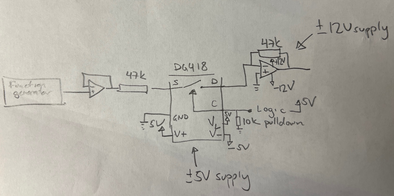
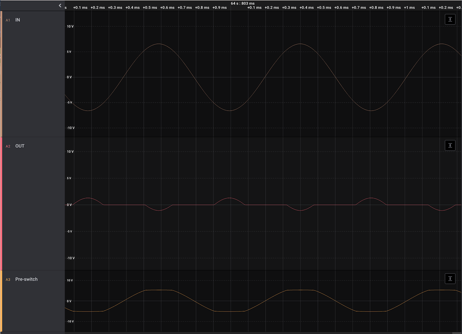
| Resistor before switch, switch off, 13Vpp. Anything above approx 5.1V is passed, giving funny little bumps on the output. |
Monday, August 7, 2023
CMOS switches and current switching
Sunday, August 6, 2023
Mix bus and channel muting
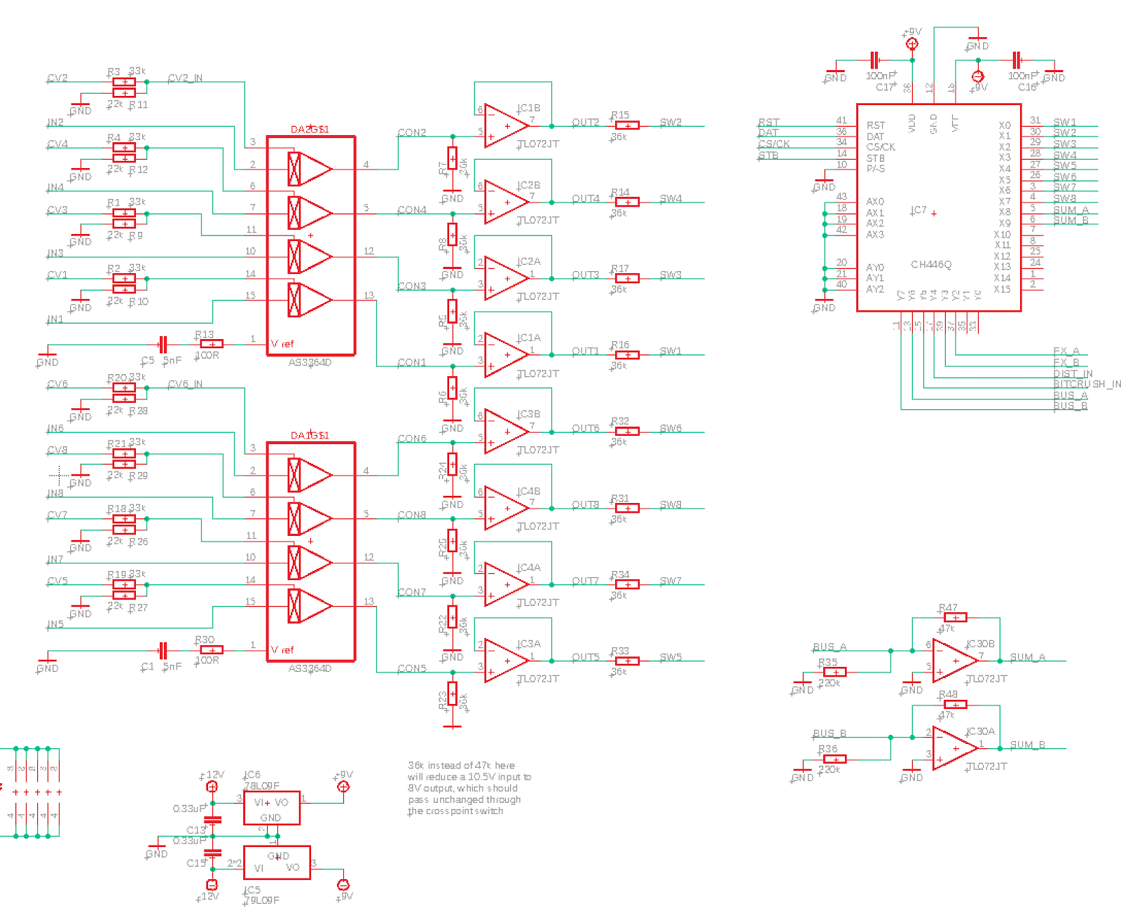
I'm designing a variation of my pre filter mixer using the CH446Q 8x16 crosspoint switch, and while doing so I started wondering if having the switch after the mix input resistor was a good thing or not.
Douglas Self to the rescue, seems that switching directly to the virtual ground of the mixer summer is the way to go.
| From "Self on Audio" by Douglas Self - Figure A seems to be the way to do things which is what I've done in my new design. |
| My mixer |
Sunday, July 23, 2023
I don't understand how to use AP
Sunday, July 9, 2023
JP6 gain through cell 2
Saturday, July 8, 2023
JP6 All-pass - inverting BP
JP6 All-pass tested
I've breadboarded and tested the AP-filter from my all-pass simulation, version AP-C: https://atosynth.blogspot.com/2023/04/jp6-filter-allpass.html
It only required minor tweaks.
During testing, my BP outputs +/-3.5V and the HP/LP outputs +/-5.2V. I assume that BP is affected the same way HP/LP is by the resonance feedback, so adjusting feedback so that HP/LP are normally +/-5V probably also affects BP amplitude.
Anyway, to get AP we need to mix 2x BP with the inverted input. But the BP needs to be unity gain.
If we assume that unity gain is +/-5V when properly adjusted, it is 5.2 when HP/LP is 5.2. That means that to bring it up from 3.5V to 5.2V we need a gain of 1.48. The simulated circuit has a gain of 1.33 when using a 100k/33k combination. Replacing the 100k with 68k gives us the gain of 1.48 that we want.
Here is a video of turning the cutoff CV knob, see how the phase changes.
The resulting circuit is like this:
PS: We need to sum everything BEFORE it reaches the filter as we need input both for AP and normal input. But this affects the polarity of the input and probably also the feedback circuit.
PPS: I am not sure how we can use AP/Phasing. Do we need to be able to pan wet/dry to different channels? Should this be an option anyway for filter outputs?
Update: Here is an alternative circuit, the AP output phase is 180 degrees different from the one above but it saves one op amp that can be used to sum stuff before the filter
Friday, July 7, 2023
New measurements with JOVE CV generation and working Cell 1 and 2
Thursday, July 6, 2023
JP6 filter oscillations and latch-up
Sunday, June 11, 2023
JP6 vs Jove revisited
Resonance
My simulation doc says the following about calibrating resonance CV:
Tune U30 until you get -125uA Reso I_abc per OTA (or to freq response is OK)
Tune U31 until you get -25uA or -4uA Reso I_abc per OTA (for similar response to 5 or 10V CV on the JP6)
Comparing to the Jove reso circuit, this is exactly what you get from trimmer extreme, -120uA to -4.2uA, so a range of -120uA to 0uA is what we want to be able to trim from software
In the following, the three lines correspond to min, center and max trimmer settings:
![]() |
| Jove resonance - voltage seen at expo converter input |
![]() |
| Jove resonance 0-10V - I_abc in single 18k resistor |
![]() |
| Jove resonance 0-5V |
![]() |
| Jove resonance 0-5V, center trim only |
![]() |
| Jove resonance response, 0V but trim min center max |
![]() |
| Jove CV response 0, 5 and 10V CV |
![]() |
| My own JP6 filter resonance I_abc. It has the same range as the Jove one but is of course not exponential, as this happens in software instead. |
![]() |
| My resonance CV circuit |
![]() |
| The Jove resonance circuit |
Cutoff
Untrimmed, Jove maxes out I_abc at -600uA with a CV of 7V approx.
This gives a cutoff of around 20-25kHz.
The lowest current is -15.6nA
My trimmed version gives 169nA to 1.06mA, max is at approx 6V CV which gives a cutoff at 25khZ, similar to the Jove.
![]() |
| Jove expo converter input vs input CV |
![]() |
| Jove I_abc in single 18k resistor |
![]() |
| Jove I_abc for center only, shows max I_abc at approx 7V |
![]() |
| Jove cutoff with CV 7.5V (center trim) |
![]() |
| My version, I_abc from 0-10V CV |
![]() |
| My version cutoff at around 6V CV |
Buffer
Jove uses a transistor (J112, N-channel FET) as a buffer, with a 33k to gnd. Replacing the opamp buffer in my circuit with a nmos in the simulation gave a slightly lower gain out. Changing the 33k to 22k or 47k didnt affect the amplitude.
| Input vs output of first cell using op amp buffer |
| Input vs output of first cell using nmos-buffer |
![]() |
| N-channel Mosfet buffer, pretty similar to what the Jove uses |
Saturday, May 13, 2023
Sunday, April 23, 2023
JP6 filter allpass
Since breadboarding the first cell of the JP6 filter was successfull, it's time to revisit the allpass circuit. I sort of got this working in an earlier post: http://atosynth.blogspot.com/2019/01/jupiter-6-all-pass-filter.html, but had to remove resonance feedback it seems.
I tried the same circuit in LTSpice again, mixing Bandpass output with the input tapped after the input mixer. It gives a nice phase change but the response is -10dB for the "normal" case, up to 4dB at the cutoff frequency, not very usefull.
I then realised that mixing with the input may refer to the original input, not what is seen after the mixer. However, the input at this point is inverted, so we don't get the phase reversal effect we're looking for
![]() |
| NB: Not original BP but unity gain one |
This is easily fixed by inverting with unity gain. Now we're talking. We get a flat response with a -6dB notch and the phase reversal we're after
I started thinking that this could be the best option, but the notch made me uncertain. After a bit of googling, I once again found the multimode filter pages at electricdruid. There, the following is stated:
"Phase shifters produce a notch in the frequency response by mixing this phase-shifted signal with the input, so technically they’re a type of notch filter."
Ok, so a notch is to be expected. I then found the link to "Craig Anderton's Multiple Identity Filter" article. I thought for a moment this confirmed my -6dB notch as it says -6dB notch at the end, but I mixed up notch and allpass. It is worth a closer look though.
But then I realised, what if I make sure BP output is the same as HP/LP etc, though my non-inverting amplifier, just as I did with the BP output from cell 1?
That works great!
The closeup doesn't look that great until you look at the axis. The input is just very slightly attenuated (-170mdB). Looking at all combinations together shows that it is essentially flat:
![]() |
| Red line is unity BP + inverted input |
Now, this is great news. Of course this is just a simulation, and as I have seen earlier, the actual result on the breadboard is different, but I think I have the best starting point at least - mix the inverted input with the unity gain BP and we get a good all pass version!
Saturday, April 15, 2023
JP6 filter debugging, part 1
Trying to breadboard a single cell of the JP6 filter. Here are my mods:
Errata:
R to -12V in cutoff CV input is 3.9R, should be 390k
op amp + and - are mixed up in cell input mixer
Modifications:
Skipping the part of reso generator that reverses CV, and leave out trimmers in reso circuit.
I inject resonance CV at reso gain 2 to bypass the inversion, and leave the reso bal unconnected. This makes reso CV go from 5 to 0 instead of 0 to 5. I use a 27k input resistor. (TODO: Why did I do that again? plot in simulation looks good at least. Probably what it was set to before removing the CV reversing and stuff in LTspice).
The cutoff CV mixer has an error (3.9R instead of 390k to gnd), so instead of using it i use the reso input mixer and a 330k to -12V on the input, still leaving balance floating. I then connect the output to a 20k trimmer, set at approx 6k (8k really, but in simulation it is 6k) and connect the output to cutoff track 2, bypassing the cutoff CV mixer.
Reso CV is set to 5V by using a resistor divider - 100k on top and 68k + 3k3 = 71k (should have been 71.4k).
Input to the cell: The input mixer is fucked up here too, I flipped it so + and - are mixed up. I use an external op amp instead, with a 33k feedback and a 100k input resistor. The output is fed to the in+ (pin 2) of the cell.
NB: SOMETHING IS MISSING HERE! pin 4 should be connected to pin 2. Anyway:
Now I can see that all three modes working - LP, BP and HP, though the input is weak and BP never really cuts off much. Next up is re-adding pin 4:
Aaaah, much better!
This time output at LP/BP/HP works. BP has a very soft cutoff slope but it DOES attenuate both above and below somewhat.
With 3.6k input with 5V max amplitude and cutoff CV at 0:
| HP outputs 7.1V, BP around 750mV, LP at -150mV |
With 100Hz input, cutoff at 5V:
| HP outputs -30mV, BP around 650mV and LP 7.6V |
With 100Hz input and cutoff at 0V:
| HP and LP are less, BP is at its max, which is 3.5V |
Filter sweep, CV 0 to 5V, 1kHz input:
Reso is not tested but at least cutoff seems to work fine :)
HP and LP outputs max out at almost the same level (7.1 to 7.6V) while BP is half of that. In my simulations it looks more like HP and LP are 5V max while BP is around 3.5V.
The fact that BP has a lower amplitude is to be expected. Looking at a simulation, we can see that the bandpass peak (purple) is where the HP (red) and LP (green) meet, as it is really just a combination of the two filters.
If we want to avoid a loudness drop when using BP, we can amplify the output slightly. In this case I've added a non-inverting op amp with a gain of 1 + 33k/100k = 1.33. The result is the blue line above and below.
An added bonus is that we can use the same input resistor (56k and 100k here) to the second cell (we could do this without the gain as well, it only leaves the BP at the low level). We can also tap all filter types after the mux and move the resistors to the mux output.
Next up:
Figure out if we should have the mix resistors before the cell 1 output mux or after, what gives the least amount of noise
See why we tap direct output after mux but before 100k res, shouldn't tapping be before the output resistors? or do we need to buffer the signal between? (Note: The JP6 uses this layout, with one 56k from HP and one from LP, and adds this to the 100k input, effectively using 156k input to the summer of cell 2).
Check output polarity from cell 1, including notch.
Tuesday, March 28, 2023
JP6 filter resonance CV
I'm testing the component based JP6 filter on a breadboard. I have some initial problems getting it to work, but then I realised that resonance is probably turned up way too high.
This made me take a look at how I generate the CV and how it affects the circuit.
This is the current circuit. The reason it is so large is that the resonance works backwards, feedback is needed to stop resonance rather than introduce it, so the CV is inverted from 0-5V to 0- -5V, then moved up 5V to get the correct response:
| CV (V) | I_abc (uA) | V_abc (V) | V_tran (V) |
| 0 | -126.0 | -13.38 | -12.11 |
| 1 | -101.7 | -13.39 | -12.37 |
| 2 | -77.0 | -13.40 | -12.6 |
| 3 | -52.0 | -13.42 | -12.9 |
| 4 | -27.5 | -13.46 | -13.18 |
| 5 | -2.7 | -13.58 | -13.55 |
Measurements again - the results are similar to the previous ones, just reversed
| CV (V) | I_abc (uA) | V_abc (V) | V_tran (V) |
| 0 | 0 | -14.3 | -14.28 |
| 1 | -24.8 | -13.46 | -13.2 |
| 2 | -49.5 | -13.42 | -12.9 |
| 3 | -74.3 | -13.40 | -12.7 |
| 4 | -99.0 | -13.40 | -12.4 |
| 5 | -123.8 | -13.38 | -12.14 |
It is interesting to note that the max current is so low (125-ish uA). It probably means that no change to the R_abc (which is 2 x 10k now) when switching to 12V supplies, though that has to be tested.
Monday, March 20, 2023
A bit about how think about the basic operation of the LM13700
It's really hard to find any absolute truths about how to design for the LM13700 as the formulas available are not possible to use directly. Thus, most people end up simulating or experimenting until they get the desired results.
This post tries to give a few good starters for the most basic cases - using the LM13700 as a simple VCA without any feedback etc. Using the details here will get you in the ballpark of what you need, without being perfect. You then have to try various resistor values until you get what you need.
Maximum values from the datasheet
- I_abc: 2mA
- I_d: 2mA
- V_differential: +/-5V
Facts (of the not so fun type)
The relationship between I_abc and gain is independent of supply voltage, BUT:
- I_d is directly proportional to supply voltage so the circuit generating it must be changed if changing supply voltage.
- The voltage at the I_abc input changes with supply voltage, so HOW I_abc is generated changes if it does not come from an ideal constant current source.
- Using the linearising diodes allows you to use a much higher input signal without distortion. A higher input means better signal-to-noise ratio, e.g. less noise on the output.
Design stuff
- I_abc and I_signal should be as large as possible (for reduced noise), within the max/design limits.
- When using the linearising diodes, I_signal can be much larger.
- I_abc goes through and sets up a voltage across R_abc. This has to follow Ohm's law, and so R_abc must be picked so that the voltage across can be large enough to hold up V = R* I for the I we want. It should not allow more than 2mA (I = V/R), any higher and the LM13700 self destructs. A bit of a safety margin is good, so maxing out at 1.8mA is fine. When switching from a 15V to 12V supply, R_abc must be reduced accordingly to allow the same I_abc range.
- The voltage at the I_abc input is said to be two diode drops above the negative rail: V_abc = 2*V_be + V-. As a diode drop is approximately 0.7V, using a 15V supply we should expect a voltage of 1.4V -15V = -13.6V
- In my simulations I've found this to be approximately true but it seems to change a little bit (around 0.5V) with control CV. It IS however consistent between 12 and 15V, with V_abc for 12V aways being 3V lower than for 15V.
- When using the linearising diodes, gain is propotional to I_d.
- Try to keep I_d = 1mA
- I_d is calculated as (+V - 0.7V) / R_d, for example, for 15V supply and 13k R_d, I_d = 14.3V / 13kOhm
- As I_d is not constant (it changes slightly with signal input), this will not always be the exact current, but it will give the correct relationship between I_d for 12 and 15V supplies
- Keep | I_s | < I_d / 2 - I_s is signal input current, but it's not evident exactly what that means, see more about the missing/wrong formula for gain below
- Differential input voltage must be < 60mV_pp (peak to peak) to keep THD < 0.1%.
- I am again not entirely sure what this means, but the datasheet uses an example with a 30k input resistor and a (trimable) 500R resistor to ground, and says that "the input divider in the input will reduce the 1Vp to 33mVpp. A simple resistor divider with 30k on top and 500R at the bottom will reduce a 2Vpp to 33mVpp so it may very well be just that, meaning that whatever input you have must be divided down so that it is at max 30Vp (single peak) or 60Vpp, ignoring any DC offset.
- I don't understand how to select resistors to connect to +in and -in, but the norm is to use a 1k pot between the inputs with the center tied to GND.
- This makes it possible to trim out DC offset/CV bleedthrough from the output.
- If the output coupled (AC coupling removes any DC component so any slight mismatch/off-centering will disappear) two 510R to GND can be used instead.
- Output current (and thus gain) when using linearising diodes can be approximated as I_o = I_g * I_abc / I_d
- I_g is the current in the input resistor and is approximated as V_in / R_in
- I_d is current into the diode biasing input and is (Vsupply - 0.7) / R_d
- The approximation is around 10-20% wrong
- Output current when NOT using linearising diodes is I_out = V_in * q * I_abc / 2kT.
- V_in is the differential voltage between the positive and negative inputs
- k is the Boltzmann constant
- q is the electron charge
- k is the ambient temperature in Kelvin
- q/kT = 38.7 V^-1 at 25C (yay, temperature dependence!)
- A good approximation for V_in is to use the voltage at the resistor formed by R_in and R_g, the resistor from the input to ground: V_diff = V_in * R_g / (R_g + R_in)
- The approximation is just 1-2 percentage points wrong compared to the simulated results, but the simulated results are 10-15% different than the calculated output. The real life results may be even more different.
- The calculated current is for an AC-coupled output. In reality, the output has a DC component, meaning it is not centered. The resistors to ground lessens this effect. Adding a DC voltage to the input can also center the output.
- Output current is converted to a voltage by sinking it to ground and buffering the output. The output voltage is then V_out = I_out * R_out
Changing supply voltages
- The voltage at the I_abc input is said to be two diode drops above the negative rail: V_abc = 2*V_be + V-. As a diode drop is approximately 0.7V, using a 15V supply we should expect a voltage of 1.4V -15V = -13.6V
- I = (Vsupply+ - 0.7V) / R_d
- The reference current resistor to get the same reference current: I_ref = Vsupply- / R_ref
- The offset voltage resistor is connected to Vsupply and must be recalculated
- R_abc must be changed to allow a smaller (when going from 15V to 12V) resistor to pass the same I_abc
A bit of background
Formulas
Without an R_d/I_d:
- gain is said to be q * I_abc / 2kT. My simulations show that it is close to what the simulator says.
- kT/q = 26mV at 25C
- however, this is only an approximation for small differential input voltages. How small? Not sure, I can't find it even though I thought I read it in the datasheet.
- and you need the differential input voltage, but that can be approximated as described above.
With R_d/I_d:
- gain is said to be I_out = I_s * (2*I_abc / I_d), for | I_s | < I_d / 2
- however, nobody really knows what that means exactly, and what I_s is it seems.
- Iain from Lushprojects (http://lushprojects.com/blog/2012/08/lm13700-missing-forumla/) came up with an alternative formula: I_out = I_g * I_abc / I_d, where I_g is the current in the signal input resistor. It is said to be around 12% less than the actual gain but gives a ballpark at least.
- I_g can be approximated as V_in / R_in, in other words ignoring that the input is not at 0V.
- The error in the formula is larger the smaller the biasing resistors get (and the smaller the input resistor gets), simply because the current in the biasing resistor increases relative to the input current. For the normal 500R biasing resistors, the error is around 17-19%.
- The error in the formula are supply voltage independent.
The takeaway from these formulas are that the gain is dependent on I_d and that you can use a bigger input signal when using I_d, meaning less noise.
Links about the wrong formula:
- http://lushprojects.com/blog/2012/08/lm13700-missing-forumla/
- https://modwiggler.com/forum/viewtopic.php?t=65783
- http://lushprojects.com/circuitjs/circuitjs.html?startCircuit=ota-gain.txt
A bit about the internals
Internally the circuit consists of four current mirrors and a differential transistor pair.
A current mirror is a circuit that makes sure that the current in two of its legs stays the same - one is the reference and one is the output - independent of what is connected to its output.
For this circuit, one of the mirrors makes sure the sum of the currents through the differential transistors, I_4 and I_5 here, equals the control current I_abc.
The three others bounces I4 and I5 around and combines them at the output, with the result being that I_4 + I_5 = I_abc
When trying to understand the circuit, it is useful to separate the analysis into two parts - what happens without any external AC input, and what happens with ONLY the AC input - as there will be a DC offset both at the input and output terminals.
Also, it helps to think about what voltages and currents are significant and what can be ignored/expected to be fairly equal.