Friday, August 18, 2023

Output phase, SVF Cell 1 and 2

Cell 1


LP, BP and HP are in phase with the filter input (which is NOT the cell input, but IS the summing point for feedback).

Notch, however, is reverse before and after the notch point. This means it will not work with feedback. I address this further down in this post.

Allpass is in phase before and after the cutoff frequency, and 180 degrees off at the cutoff frequency. I am not sure if this is wrong and has to be corrected, I need to check the expected behaviour, though I believe that adding AP and dry should give a notch, which is what would happen here as the 180 degrees off at cutoff would cancel out the dry signal.

Cell 2
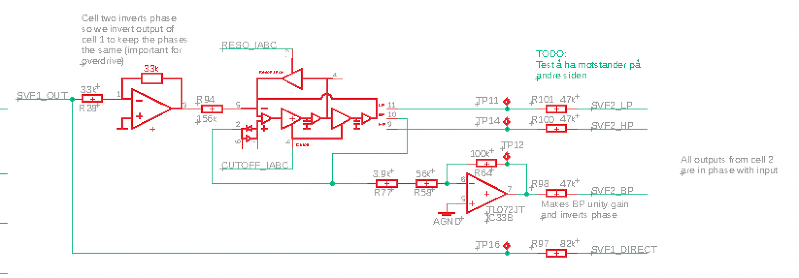
Cell 2, all outputs are in phase with input


The outputs of Cell 2 (as seen by the mux) is in phase with its input (Holds true for LP, BP and HP, and of course for the Cell 1 direct as this is the same as the input to Cell 2).

The op amp after the mux inverts the signal so the output phase of the filter is inverted. 


This affects both the output itself and the filter feedback. The output phase is selectable so that's taken care of there. The feedback on the other hand, is inverted back in the feedback VCA (positive input + inverting op amp).

Feedback VCA inverts signal

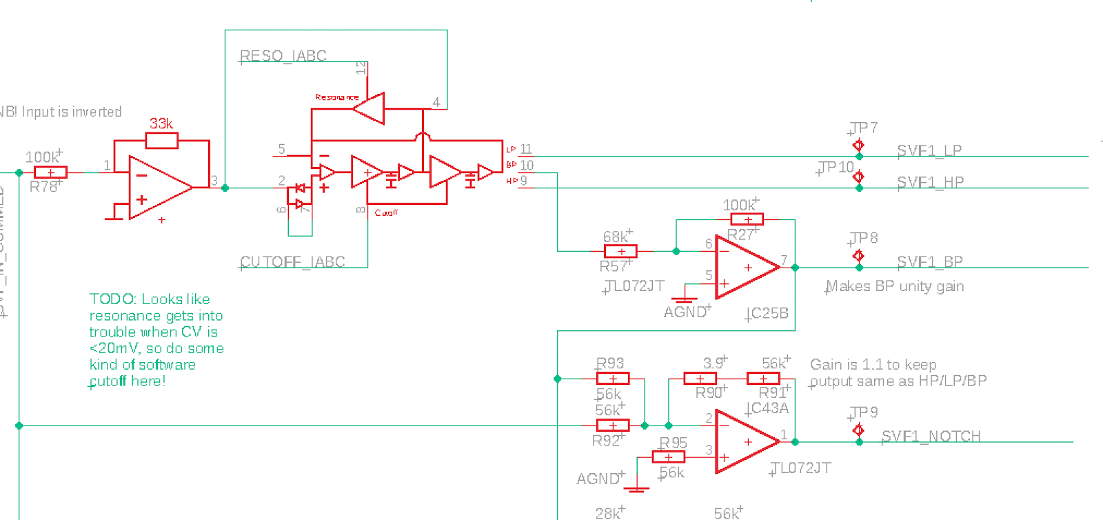
Alternative notch

Combining dry (inverted) and BP (unity gain) can give me notch without having to add another op amp (as described here: http://atosynth.blogspot.com/2019/01/jupiter-6-all-pass-filter.html)


Simulating this shows a big difference in the offness of the notch - green is LP + HP, red is dry + BP.


From the simulation, LP + HP results in a -1.2dB down to -36dB notch. Dry + BP results in -19.5dB.


Measured in my circuit I see approx +/-150mV for LP+HP, though it looks a bit noisy. Dry + BP is +/-375mV.


Also, gain when no notch is a little low:


The output is +/-5V. To boost it to +/-5.5V which is the range of the other waveforms, we can use 56k + 3.9k in op amp feedback, making the gain 1.07

Here is the alternative notch circuit:


Thursday, August 10, 2023

Output levels, SVF Cell 1 & 2

Cell 1

I've measured the output levels of three different circuits for cell 1 of the SVF.

The results are fairly stable, within approx 0.05-0.1V between cells.

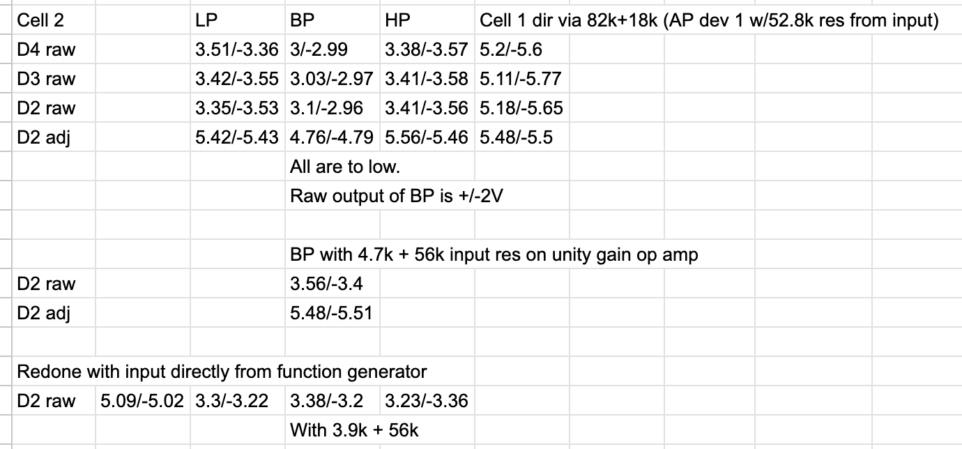
Output of LP, BP, HP and Notch are all around +/-5.5V when input is +/-5.0V. 

As I mix BP with input, and the output should be 2 x BP + Input, we have to reduce the input resistor for input to boost it from 5 to 5.5V approx. 

BP output is between +/-5.3 and +/-5.4 for all cards, so gain needs to be between 5.3/5 = 1.06 and 5.4/5 = 1.08 Experimentiation showed that using a 51k and 1.8k resistor in series, combined with the 56k feedback resistor, gave a good result. The calculated gain for this is 1.06.


Cell 2

I did the same for Cell 2, testing device 2, 3 and 4 against each other, and again they match fairly well.

Raw output is around +/-3.4V with a little offset. BP, however, was too low even after the 100k/67k boost and came out around +/-3V. After some experimenting I chose to replace the 67k resistor with 4.7k + 56k, which brought BP up to the same as the others.

The output after final amplification is +/-5.4 to 5.5V which is approx the same as from cell 1. Not sure if I should adjust this back to +/-5V, as the input is 5V, I guess unity gain is a nice feature so perhaps worth the extra work.


Monday, August 7, 2023

CMOS switches and current switching

After my previous post where I discovered that Douglas Self has some examples where he's switching mixer inputs at the op amp virtual ground, and after talking to the guy on Reddit that made me discover the CH446Q (ARabidSquid, Architeuthis Flux on Tindie), I decided to test it in practice.

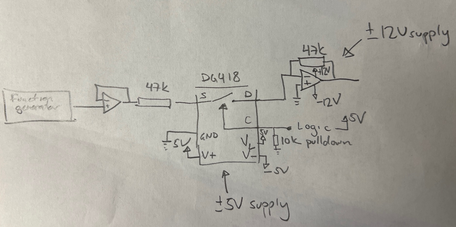
I hooked up a DG418 on a breadboard, and used an 78L05 and 79L05 to get a +/-5V supply for the DG418.

I then used a TL072 op amp with +/-12V supplies, with one op amp to buffer the input from the function generator and the second to "sum" (just invert really) the output from the switch, with a 47k negative feedback resistor. 

Version of circuit where input resistor is before the switch


I could now experiment with having the op amp input resistor BEFORE the switch (placing the switch at the virtual ground) or AFTER the switch

An initial test with a 10Vpp (+/-5V) signal showed that it worked in both configurations.

Resistor after the switch, 10Vpp

Resistor before the switch, 10Vpp


I then placed a 20Vpp signal on the version with the resistor after the switch. As expected, the switch clips the signal since it sees the full 20Vpp, but exactly how it clips is interesting. Measured at the input pin (i.e. the output of the buffer), the INPUT is clipped - the top is at 9.16V and the bottom at -5.85. I didn't expect it to be asymmetrical.

Resistor after the switch, 20Vpp. Output (and input) clips


Next up, I moved the resistor to before the input. The switch should now see no voltage swing (though a current passes through, +/-0.2mV at its peaks). This also worked as expected, the output is also 20Vpp (though inverted because of the op amp configuration).

Resistor before switch, 20Vpp passes nicely


This looked very promising. Next up was turning the switch OFF. 

Again, for the 10Vpp signal, it worked as it should for both variations.

Switch off, 10Vpp


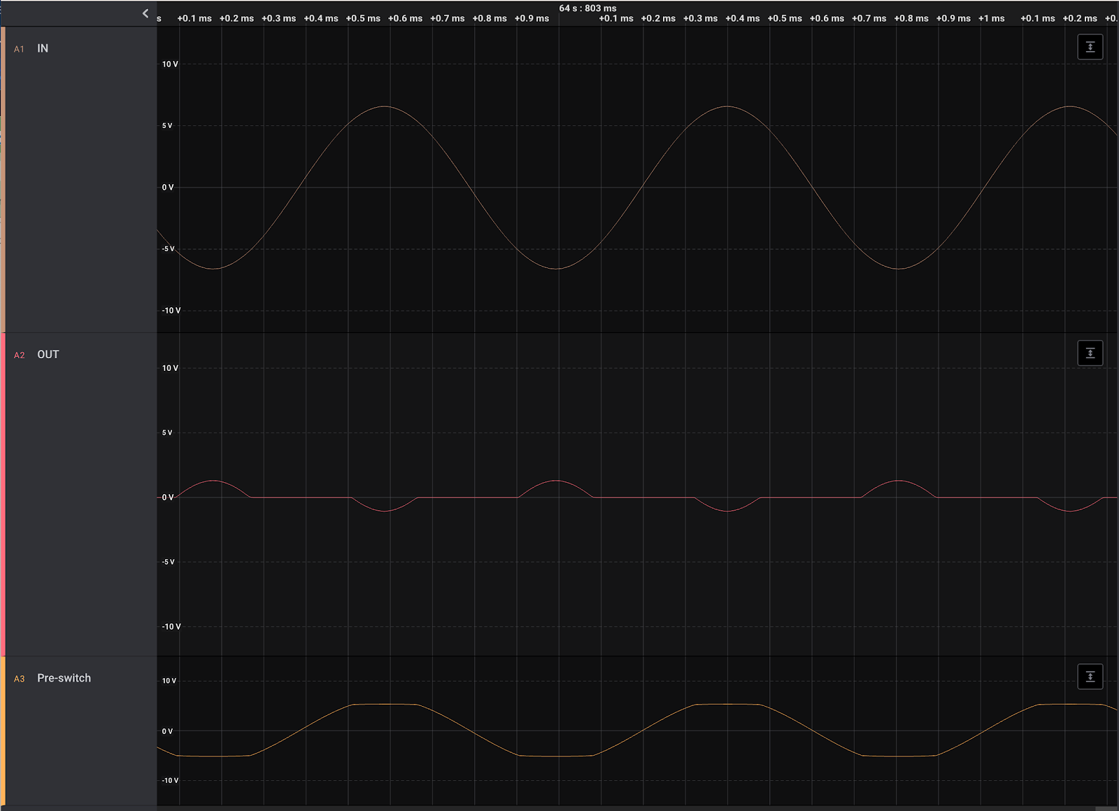
I then tried cranking up the signal for the variation with the resistor before the switch, but then "disaster" struck: Once the input signal got higher than the DG418's supplies, it started leaking! With a 13Vpp input, it blocked everything up to 10Vpp. The remaining, however, was passed through, giving the output small "bumps"! 

Resistor before switch, switch off, 13Vpp. Anything above approx 5.1V is passed, giving funny little bumps on the output.


When showing the result to ARabidSquid, he confirmed that this was how CMOS operate, it cannot block anything higher than it's supply voltages.

After seeing this result, I remembered that I read something similar yesterday - someone posted about a similar issue, where a current input made the switch leak when it was turned on. Someone suggested using an SPDT (or two switches in a crosspoint switch) to sink the current. This could be an option, to use a separate bus to sink all input signals that are not in use. However, I think I'd rather stay within the operating limits and keep my signals at 16Vpp max.

Sunday, August 6, 2023

Mix bus and channel muting

I'm designing a variation of my pre filter mixer using the CH446Q 8x16 crosspoint switch, and while doing so I started wondering if having the switch after the mix input resistor was a good thing or not. 

Douglas Self to the rescue, seems that switching directly to the virtual ground of the mixer summer is the way to go.

From "Self on Audio" by Douglas Self - Figure A seems to be the way to do things which is what I've done in my new design.

My mixer


Sunday, July 23, 2023

I don't understand how to use AP

Now that the AP is working properly on the JP6 filter, I'm trying to understand how to use it.

Most places say that you should mix it with the original signal, but when I do that I get exactly what I get from my notch:

Red: Notch. Blue: 50% AP + 50% Dry


Sunday, July 9, 2023

JP6 gain through cell 2

In the simulation, cell 2 outputs a +/- 2.6V signal when output from Cell 1 is 4V. This in turn arrives at the output as 3.1V and is overdriven to 4V with a nice rounded shape. 

Now, the output gain feedback resistor is 100k. Let's do some calculations.

LP and HP are tapped through 33k + 47k = 80k. That should give a gain of 1.25, which should give an output of 2.6 * 1.25 = 3.25.

The output of the BP requires a gain of 1.33 in cell1 in the simulation, and 1.5 on the breadboard, to be equal to the LP and HP outputs

That means a total gain of 1.25 * 1.33 = 1.66 (or 1.88 on the breadboard)

Thus, we need 100k / x = 1.66, x= 60k (or 53k for the breadboard).

For the direct output from cell 1, which is at 4V in the simulation, to get it to 3.1 requires a gain of 3.25/4 = 0.81, or a 125k input resistor. 

Now, wait a minute. Gain < 1 is generally not something we do, we usually do it by using a resistor divider. But let's not, let's rise the output level from 3.25 to 4 instead, meaning we only need unity gain for cell 1.

That gives us the input resistor for LP/HP as

gain = 4/2.6 = 1.54, R = 65k

and for BP

gain  = 1.33 * 1.54 = 2, R = 50k (and 1.5 * 1.54 = 2.3, r = 43.5)

Let's see what this does in the simulation:

Well, LP still looks good, at just a tad below 4V. Then, turning up overload to max fivces a slightly more distorted wave, but still cool, and with an amplitude of 5.1.

Now for another check, what happens with a 20Vpp signal. Does it distort?

It definitely does, but that's not because of the feedback, it's just how the circuit works.

We could get around this by using a 200k input resistor instead of a 100k, and then double the gain at the end of the circuit instead. We'll just have to try this to see how it affects both a 5V and 10V signal when doing distortion.

On breadboard

I tried sending a 5V signal through cell 2, and I get 3.23V on LP, 3.32V on HP and 2V on BP, meaning we need a gain around 1.6 for BP. 

To get all up to 5V at the output would require gains of
HP/LP: 5 / 3.23 = 1.54
BP: 5 / 2 = 2.5
and unity.

100k / 1.54 = 65k
100k / 2.5 = 40k

So a combination of 47k and 18k, and 22k and 18k is a good starting point.

Testing: 
LP: Near perfect 5V out
HP: Output is 5.2V, so a tiny bit too high
BP: Damn close to correct.


This means I will try the following for cell 2 in "production":
HP and LP: 47k +18k
BP: 22k + 18k
Direct: 82k + 18k

For cell 1 I will use 56k for everything, but BP is boosted by 1.5 using a 150k feedback and 100k input resistor


Next things to try on breadboard:
- overdrive
- no resistor pre-mux for cell 1
- swap cells to see if they behave similarly
- output vca.
- polaritites for output VCA and overdrive, see if we should modify cell circuit

See "Jupiter 6 filter - no VCA - 12V - JOVE trials -overdrive"


Saturday, July 8, 2023

JP6 All-pass - inverting BP

In my simulations and breadboarding I added an inverting op amp for the input to get AP. But what if we instead inverted BP? It is already 180 degrees off compared to HP and LP. 

I simulated this, and it looks like it works well. Instead of going from -360 to 0 degrees it goes from -180 to 180, which is just to say that the output is inverted compared to the input - just like HP and LP.

As I'm already planning on having an invert button/switch on the SVF this doesn't matter :-D 

It also saves me one opamp.

As for the opamp gain, to keep the gain at 1.48 (or 1.5, it probably doesnt matter too much) we can go with 100k input and 150k feedback, or 68k/100k.

I will try this now.

JP6 All-pass tested

I've breadboarded and tested the AP-filter from my all-pass simulation, version AP-C: https://atosynth.blogspot.com/2023/04/jp6-filter-allpass.html

It only required minor tweaks.

During testing, my BP outputs +/-3.5V and the HP/LP outputs +/-5.2V. I assume that BP is affected the same way HP/LP is by the resonance feedback, so adjusting feedback so that HP/LP are normally +/-5V probably also affects BP amplitude.

Anyway, to get AP we need to mix 2x BP with the inverted input. But the BP needs to be unity gain.

If we assume that unity gain is +/-5V when properly adjusted, it is 5.2 when HP/LP is 5.2. That means that to bring it up from 3.5V to 5.2V we need a gain of 1.48. The simulated circuit has a gain of 1.33 when using a 100k/33k combination. Replacing the 100k with 68k gives us the gain of 1.48 that we want. 

Here is a video of turning the cutoff CV knob, see how the phase changes.


The resulting circuit is like this:


PS: We need to sum everything BEFORE it reaches the filter as we need input both for AP and normal input. But this affects the polarity of the input and probably also the feedback circuit.

PPS: I am not sure how we can use AP/Phasing. Do we need to be able to pan wet/dry to different channels? Should this be an option anyway for filter outputs?


Update: Here is an alternative circuit, the AP output phase is 180 degrees different from the one above but it saves one op amp that can be used to sum stuff before the filter


Friday, July 7, 2023

New measurements with JOVE CV generation and working Cell 1 and 2

NB: R_abc is 10k instead of the 18k found in the JOVE circuit.

Resonance

I think the resonance looks quite good

Here are some quick measurements of the resonance voltages using the JOVE resonance circuit. This seems to give approxmiately unity gain for HP/LP and self resonance (could perhaps be a bit better).

Output of trimmer 1: -2.83V
Output of trimmer 2: -10.83V

Reso CV: 0V
Output CV mixer: 2.9V
Base voltage: -52mV

Reso CV: 5V
Output CV mixer: 7.94V
Base voltage: -10mV

Cutoff

The cutoff range seems too limited, but with this, a 50Hz wave has an amplitude of approx 130mVpp. At max, the HP filter lets a 1.5kHz wave through with 180mVpp. An 8k wave has approx 5Vpp amplitude.

Cutoff trimmer 1: -8.4V

Cutoff CV 0:
Output CV mixer: 998mV
Base voltage: 100mV

Cutoff CV 5:
Output CV mixer: -1.25V
Base voltage: -100mV

Polarities
LP output, Cell 1: inverted
BP output, Cell 1: normal
HP output, Cell 1: inverted

Amplitudes 
HLP Max: +/-5.25V
BP Max: +/-3.5V
HP Max: +/-5.25V

High frequency oscillations
The high frequency oscillations seen previously are completely gone (though I have not tested with higher CV), perhaps they were caused by the erroneous 3p filter cap

Thursday, July 6, 2023

JP6 filter oscillations and latch-up

I've had serious troubles with the JP6 filter since I started working on it again about a week ago.

- it latched up whenever the cutoff CV was > 1.5V
- it had severe high-frequency oscillations

Today, I finally got it working again (with the Jove CV generation circuits). Here are the three things I fixed:

- Cutoff and Resonance Iabc has to go to two cells, not only one (or they will be too large)
- I had messed up and used a 3pF instead of a 330pF cap
- And even after fixing that, I realised that the caps were probably not in contact with the connectors. I redid the wiring there and everything started working.

Back to the real testing!

Sunday, June 11, 2023

JP6 vs Jove revisited

As part of getting my JP6 filter working, I thought it would be a good idea to revisit the Jove JP6 filter (https://system80.net/product/jove/https://github.com/minisystem/JOVE) to compare it to what I'm doing. It is especially interesting to see how the control signals differ, and what their ranges are.

The conclusion is that everything is very similar and my control signals cover the Jove signal ranges - but it is worth mentioning that the cutoff maxes out at around 23kHz on the Jove.

Here are my findings in detail:

Resonance

My simulation doc says the following about calibrating resonance CV:

Tune U30 until you get -125uA Reso I_abc per OTA (or to freq response is OK)

Tune U31 until you get -25uA or -4uA Reso I_abc per OTA (for similar response to 5 or 10V CV on the JP6)

Comparing to the Jove reso circuit, this is exactly what you get from trimmer extreme, -120uA to -4.2uA, so a range of -120uA to 0uA is what we want to be able to trim from software

In the following, the three lines correspond to min, center and max trimmer settings:

Jove resonance - voltage seen at expo converter input

Jove resonance 0-10V - I_abc in single 18k resistor


Jove resonance 0-5V

Jove resonance 0-5V, center trim only

Jove resonance response, 0V but trim min center max


Jove CV response 0, 5 and 10V CV

My own JP6 filter resonance I_abc. It has the same range as the Jove one but is of course not exponential, as this happens in software instead.

My resonance CV circuit

The Jove resonance circuit


Cutoff

Untrimmed, Jove maxes out I_abc at -600uA with a CV of 7V approx.

This gives a cutoff of around 20-25kHz.

The lowest current is -15.6nA


My trimmed version gives 169nA to 1.06mA, max is at approx 6V CV which gives a cutoff at 25khZ, similar to the Jove.

Jove expo converter input vs input CV

Jove I_abc in single 18k resistor

Jove I_abc for center only, shows max I_abc at approx 7V

Jove cutoff with CV 7.5V (center trim)

My version, I_abc from 0-10V CV

My version cutoff at around 6V CV


Buffer

Jove uses a transistor (J112, N-channel FET) as a buffer, with a 33k to gnd. Replacing the opamp buffer in my circuit with a nmos in the simulation gave a slightly lower gain out. Changing the 33k to 22k or 47k didnt affect the amplitude. 


Input vs output of first cell using op amp buffer


Input vs output of first cell using nmos-buffer

N-channel Mosfet buffer, pretty similar to what the Jove uses